UPD3739 Просмотр технического описания (PDF) - NEC => Renesas Technology
Номер в каталоге
Компоненты Описание
производитель
UPD3739 Datasheet PDF : 24 Pages
| |||
µPD3739
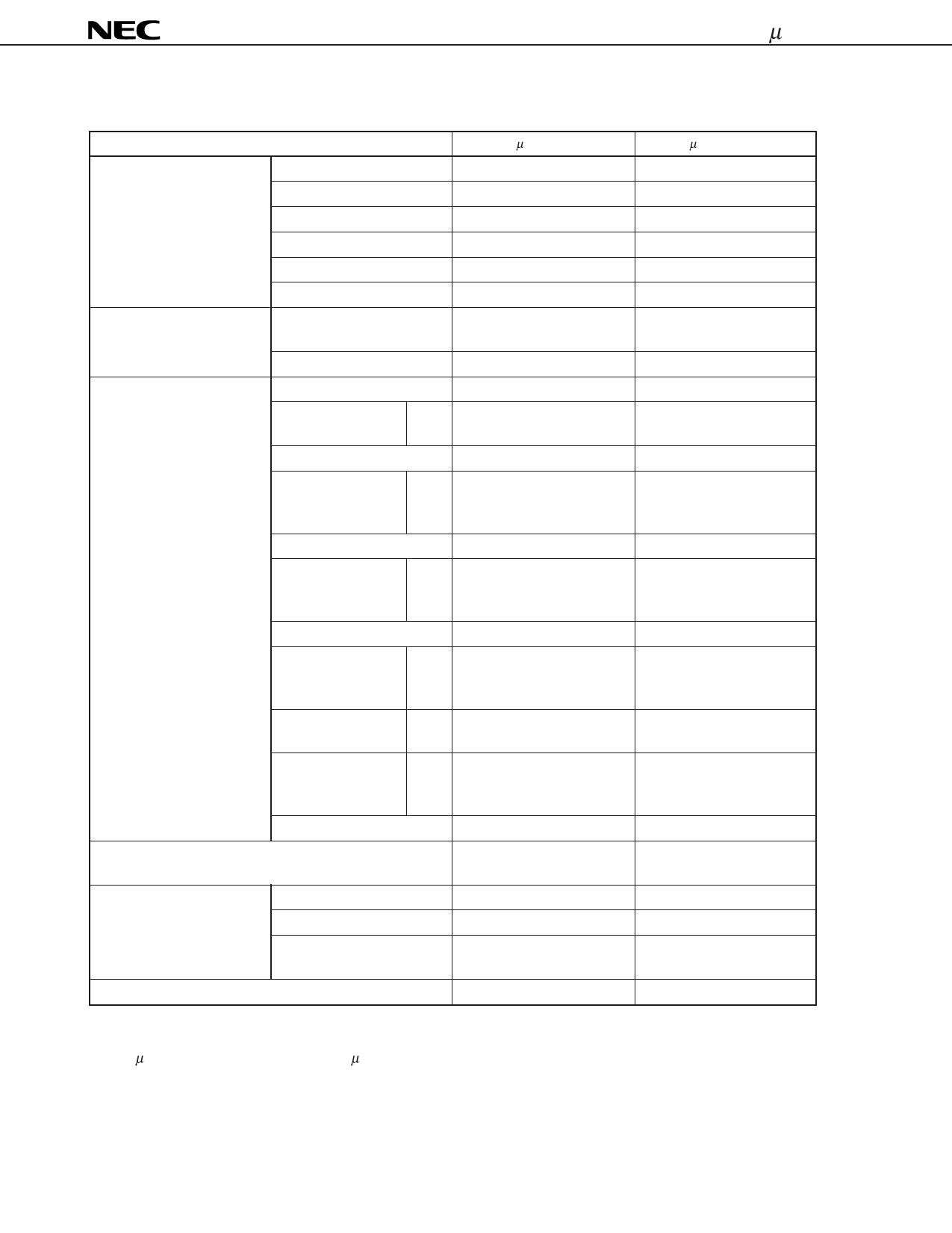
COMPARISON CHART
Item
µPD3739
PIN CONFIGURATION
Pin 1
GND
Pin 2
NC
Pin 4
NC
Pin 11
NC
Pin 21
NC
Pin 22
NC
RECOMMENDED
OPERATING CONDITIONS
Capacitance of reset gate clock
pin external capacitor (pF)
1000 ± 20 %
Data rate MIN. (MHz)
0.5
ELECTRICAL
Saturation exposure TYP. (Ix⋅s)
0.17
CHARACTERISTICS
Photo response
TYP.
4
non-uniformity (%) MAX.
10
Average dark signal TYP. (mV)
0.3
Dark signal
MIN.
0
non-uniformity (mV) TYP.
4
MAX.
6
Power consumption MAX. (mW)
400
Response (V/Ix⋅s)
MIN.
TYP.
MAX.
7.2
9.0
10.8
Offset level TYP. (V)
3.5
Shift register clock pin MIN.
250
capacitance (pF) Note TYP.
350
MAX.
500
Dynamic range TYP. DR1
(times)
DR2
375
2143
Reset feed-through MIN.
0
noise (mV)
TYP.
400
MAX.
600
Random noise TYP. (mV)
0.7
TIMING CHART
In phase outputs operating
timing is added
DEFINITIONS OF
Photo response non-uniformity Absolute value
CHARACTERISTICS ITEMS Dark signal non-uniformity
Absolute value
Random noise
Standard deviation of signal
level distribution by scan
RECOMMENDED SOLDERING CONDITIONS
Wave soldering is deleted
µPD35H71A
DGND
TEST
VDD
VSUB
AGND
DGND
Unspecified
Unspecified
0.29
±5
±10
1.0
–3
–1, +3
+6
Unspecified
4.15
5.2
6.25
3.0
400
500
800
500
Undefined
Unspecified
250
500
Undefined
Out of phase outputs
operation only
Minus and plus value
Minus and plus value
Undefined
—
Note Due to the changing of measurement conditions, and pin capacitance of each devices is almost the same.
(µPD3739: Power supply = 12 V, µPD35H71A: Power supply = 0 V)
2
Share Link: 