UPD160040 Просмотр технического описания (PDF) - NEC => Renesas Technology
Номер в каталоге
Компоненты Описание
производитель
UPD160040
NEC => Renesas Technology

UPD160040 Datasheet PDF : 19 Pages
| |||
µPD160040
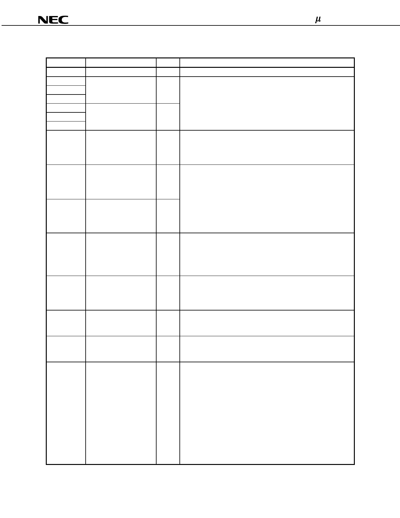
4. PIN FUNCTIONS
Pin Symbol
S1 to S384
D00 to D07
D10 to D17
D20 to D27
D30 to D37
D40 to D47
D50 to D57
R,/L
Pin Name
Driver
Port 1 display data
Port 2 display data
Shift direction control
5 STHR
Right shift start pulse
5 STHL
Left shift start pulse
CLK
Shift clock
STB
Latch
SRC
ORC
POL
Through rate control
Output resistance control
Polarity input
(1/2)
I/O
Output
Input
Input
Description
The D/A converted 256-gray-scale analog voltage is output.
The display data is input with a width of 48 bits, viz., the gray scale data
(8 bits) by 6 dots (2 pixels).
DX0: LSB, DX7: MSB
Input
I/O
I/O
Input
Input
Input
Input
Input
The shift direction control pin of shift register. The shift directions of the
shift registers are as follows.
R,/L = H (right shift): STHR input, S1→S384, STHL output
R,/L = L (left shift): STHL input, S384→S1, STHR output
These are the start pulse input/output pins when connected in cascade.
Loading of display data starts when a H level is read at the rising edge
of CLK.
A H level should be input at the pulse of one cycle of the clock signal.
If the start pulse input is more than 2 CLK, the first 1 CLK of the H-level
input is valid.
For right shift, STHR is input and STHL is output.
For left shift, STHL is input and STHR is output.
The shift clock input pin of shift register. The display data is loaded into
the data register at the rising edge.
When 66-clock pulses are input after input of the start pulse, input of
display data is halted automatically. The contents of the shift register
are cleared at the STB’s rising edge.
The contents of the data register are transferred to the latch circuit at
the rising edge. In addition, at the falling edge, the gray scale voltage is
supplied to the driver. It is necessary to ensure input of one pulse per
horizontal period.
SRC = H: High-through-rate period (large current consumption)
SRC = L: Low-through-rate period (small current consumption)
SRC is pulled up to the VDD1 in the IC.
ORC = H: Low output resistance period
ORC = L: High output resistance period
ORC is pulled up to the VDD1 in the IC.
POL = L: The S2n−1 output uses V0-V7 as the reference supply. The S2n
output uses V8-V15 as the reference supply.
POL = H: The S2n−1 output uses V8-V15 as the reference supply. The S2n
output uses V0-V7 as the reference supply.
S2n−1 indicates the odd output and S2n indicates the even output. Input
of the POL signal is allowed the setup time (tPOL–STB) with respect to
STB’s rising edge.
When it switches such as POL = H→L or L→H, all output pins are
output reset during STB = H. When it does not switch, all output pins
become Hi-Z (high impedance) during STB = H. Refer to 7.
RELATIONSHIP BETWEEN MODE, STB, SRC, ORC, POL, AND
OUTPUT WAVEFORM for details.
4
Data Sheet S15859EJ1V0DS
Share Link: