ADM101EWARMZ-REEL7 Просмотр технического описания (PDF) - Analog Devices
Номер в каталоге
Компоненты Описание
производитель
ADM101EWARMZ-REEL7 Datasheet PDF : 12 Pages
| |||
Data Sheet
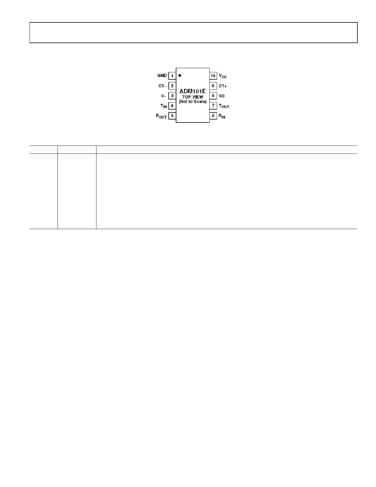
PIN CONFIGURATION AND FUNCTION DESCRIPTIONS
ADM101E
Figure 2. Pin Configuration
Table 3. Pin Function Descriptions
Pin No. Mnemonic Function
1
GND
Ground Pin. Must be connected to 0 V.
2
C1−
Negative Terminal of C1 (if C1 is Polarized Capacitor).
3
V−
Internally Generated Negative Supply Voltage.
4
TIN
Driver Input (3 V to 5 V TTL/CMOS Logic Levels).
5
ROUT
Receiver Output (3 V to 5 V TTL/CMOS Logic Levels).
6
RIN
Receiver Input (EIA-232 Signal Levels).
7
TOUT
Driver Output (EIA-232 Signal Levels).
8
SD
Shutdown Input. Logic 1 on this input puts the ADM101E into low power shutdown mode.
9
C1+
Positive Terminal of Charge Pump Capacitor (if C1 is Polarized Capacitor).
10
VCC
Positive Power Supply, Nominally 5 V.
Rev. B | Page 5 of 12
Share Link: 