UC3842A-BW Просмотр технического описания (PDF) - First Components International
Номер в каталоге
Компоненты Описание
производитель
UC3842A-BW Datasheet PDF : 10 Pages
| |||
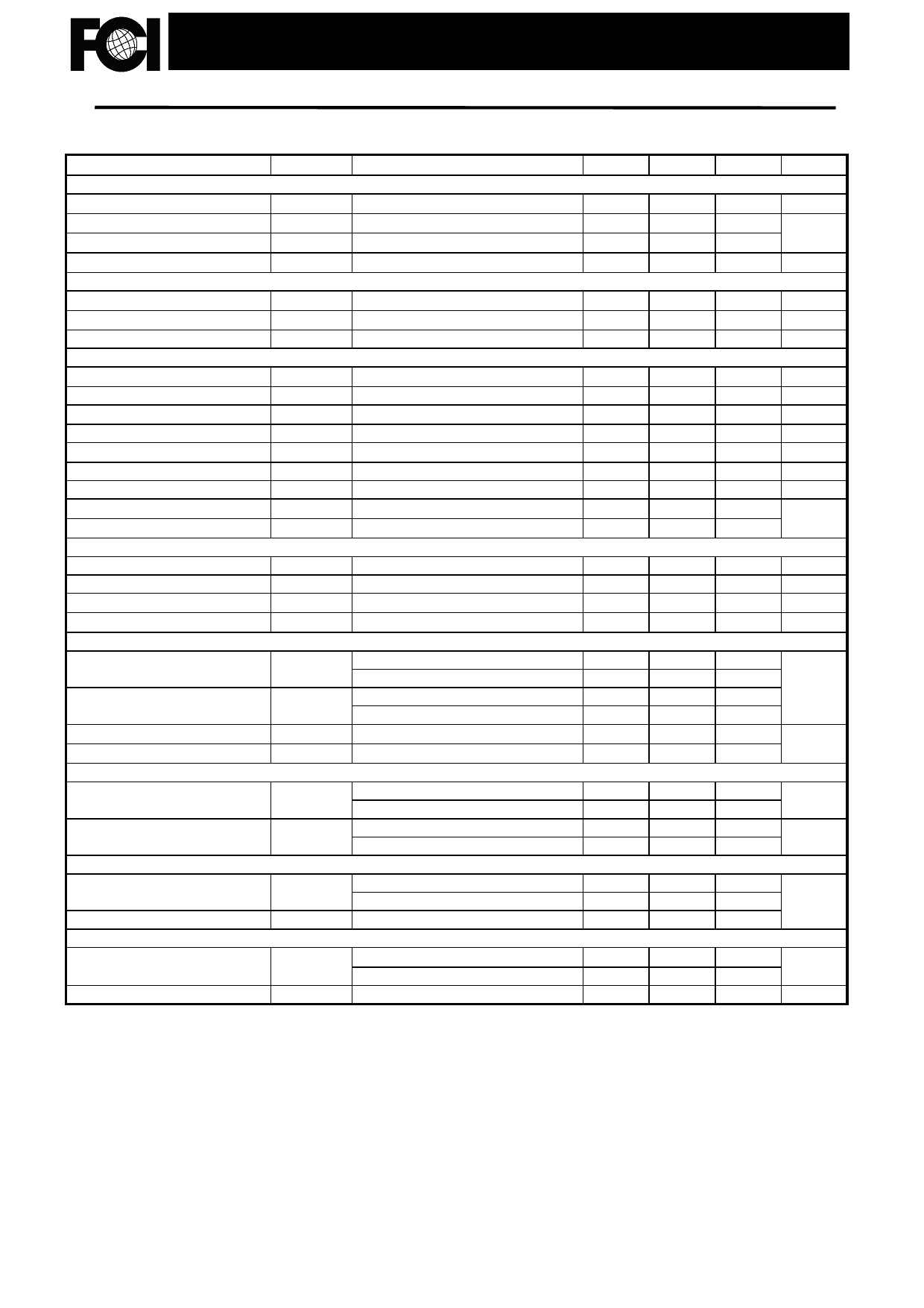
UC384XA-BW Current Mode PWM Controller
(UC3842A-BW/ 43A-BW/ 44A-BW/ 45A-BW)
Electrical characteristics (*VCC=15V, RT=10kΩ, CT=3.3nF, TA=00C to +700C, unless otherwise
specified)
Characteristics
Symbol
Test Condition
Min
Typ
Max
Reference Section
Reference Output Voltage
Line Regulation
Load Regulation
Short Circuit Output Current
Oscillator Section
VREF
∆VREF
∆VREF
ISC
TJ = 25°C, IREF = 1 mA
12V ≤ VCC ≤ 25 V
1 mA ≤ IREF ≤ 20mA
TA = 25°C
4.9
5.0
5.1
6.0
20
6.0
25
-100
-180
Oscillation Frequency
Frequency Change with Voltage
Oscillator Amplitude
Error Amplifier Section
f
∆f/∆VCC
V(OSC)
TJ = 25°C
12V ≤ VCC ≤ 25 V
(peak to peak)
47
52
57
0.05
1.0
1.6
Input Bias Current
IBIAS
VFB=3V
-0.1
-2
Input Voltage
Open Loop Voltage Gain
Unity Gain Bandwidth
Power Supply Rejection Ratio
Output Sink Current
Output Source Current
High Output Voltage
Low Output Voltage
Current Sense Section
VI(E.A)
AVOL
UGBW
PSRR
ISINK
ISOURCE
VOH
VOL
Vpin1 = 2.5V
2V ≤ V0 ≤ 4V
Tj=250C, Note 3
12V ≤ VCC ≤ 25 V
Vpin2 = 2.7V, Vpin1 = 1.1V
Vpin2 = 2.3V, Vpin1 = 5V
Vpin2 = 2.3V, RL = 15KΩ to GND
Vpin2 = 2.7V, RL = 15KΩ to PIN 8
2.42
65
0.5
60
2
-0.5
5.0
2.5
90
0.6
70
7
-1.0
6.0
0.8
2.58
1.1
Gain
Maximum Input Signal
Supply Voltage Rejection
Input Bias Current
GV
VI(MAX)
SVR
IBIAS
(Note 1 & 2)
V pin1 = 5V (Note1)
12V ≤ VCC ≤ 25 V (Note 1)
Vpin3 = 3V
2.85
0.9
3.0
1.0
70
-3.0
3.15
1.1
-10
Output Section
Low Output Voltage
VOL
High Output Voltage
VOH
Rise Time
tR
Fall Time
tF
Undervoltage Lockout Section
ISINK = 20 mA
ISINK = 200 mA
ISINK = 20 mA
ISINK = 200 mA
TJ = 25°C, CL = 1nF (Note 3)
TJ = 25°C, CL = 1nF (Note 3)
0.08
0.4
1.4
2.2
13
13.5
12
13.0
45
150
35
150
Start Theshold
VTH(ST)
UC3842A-BW/44A-BW
UC3843A-BW/45A-BW
14.5
7.8
16.0
8.4
17.5
9.0
Min. Operating Voltage
(After Turn On)
VOPR(min) UC3842A-BW/44A-BW
UC3843A-BW/45A-BW
8.5
10
11.5
7.0
7.6
8.2
PWM Section
Max. Duty Cycle
D(MAX)
UC3842A-BW/43A-BW
UC3844A-BW/45A-BW
95
97
100
47
48
50
Min. Duty Cycle
D(MAX)
0
Total Standby Current
Start−Up Current
IST
UC384XA-BW
0.17
0.3
Operating Supply Current
ICC (OPR) Vpin3 = Vpin2 = 0V
13
17
Zener Voltage
VZ
ICC=25 mA
30
38
* Adjust VCC above the start threshold before setting it to 15V.
Note 1: Parameter measured at trip point of latch with Vpin2=0.
Note 2: Gain defined as A=∆Vpin1/∆Vpin3 ; 0 ≤ Vpin3 ≤ 0.8V.
Note 3: These parameters, although guaranteed, are not 100% tested in production.
Unit
V
mV
mA
KHz
%
V
µA
V
dB
MHz
dB
mA
mA
V
V/V
V
dB
µA
V
nS
V
V
%
mA
V
2
Share Link: 