UC3842B(2013) Просмотр технического описания (PDF) - ON Semiconductor
Номер в каталоге
Компоненты Описание
производитель
UC3842B Datasheet PDF : 22 Pages
| |||
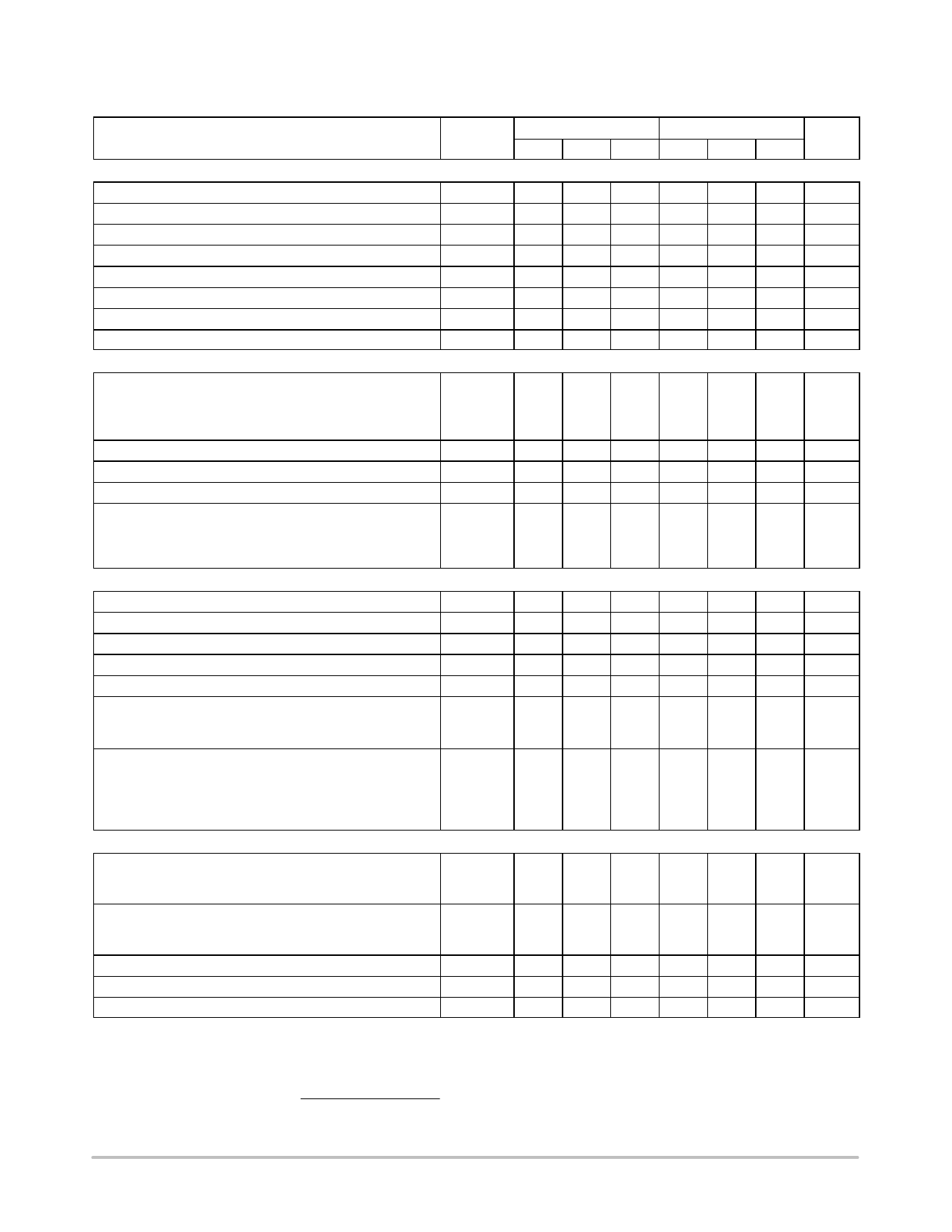
UC3842B, UC3843B, UC2842B, UC2843B
ELECTRICAL CHARACTERISTICS (VCC = 15 V [Note 3], RT = 10 k, CT = 3.3 nF. For typical values TA = 25°C, for min/max values
TA is the operating ambient temperature range that applies [Note 4], unless otherwise noted.)
UC284XB, UC2843D
UC384XB, XBV
Characteristics
Symbol Min Typ Max Min Typ Max Unit
REFERENCE SECTION
Reference Output Voltage (IO = 1.0 mA, TJ = 25°C)
Vref
4.95 5.0 5.05 4.9 5.0 5.1
V
Line Regulation (VCC = 12 V to 25 V)
Regline
−
2.0
20
−
2.0
20
mV
Load Regulation (IO = 1.0 mA to 20 mA)
Regload
−
3.0
25
−
3.0
25
mV
Temperature Stability
TS
−
0.2
−
−
0.2
− mV/°C
Total Output Variation over Line, Load, and Temperature
Vref
UC284XB
UC2843D
V
4.9
−
5.1 4.82
−
5.18
4.82
−
5.18
Output Noise Voltage (f = 10 Hz to 10 kHz, TJ = 25°C)
Long Term Stability (TA = 125°C for 1000 Hours)
Vn
−
50
−
−
50
−
mV
S
−
5.0
−
−
5.0
−
mV
Output Short Circuit Current
ISC
− 30 − 85 −180 − 30 − 85 −180 mA
OSCILLATOR SECTION
Frequency
TJ = 25°C
TA = Tlow to Thigh
TJ = 25°C (RT = 6.2 k, CT = 1.0 nF)
fOSC
kHz
49
52
55
49
52
55
48
−
56
48
−
56
225 250 275 225 250 275
Frequency Change with Voltage (VCC = 12 V to 25 V)
DfOSC/DV
−
0.2 1.0
−
0.2 1.0
%
Frequency Change with Temperature, TA = Tlow to Thigh
DfOSC/DT
−
1.0
−
−
0.5
−
%
Oscillator Voltage Swing (Peak−to−Peak)
VOSC
−
1.6
−
−
1.6
−
V
Discharge Current (VOSC = 2.0 V)
TJ = 25°C, TA = Tlow to Thigh
UC284XB, UC384XB
UC2843D, UC384XBV
Idischg
mA
7.8 8.3 8.8 7.8 8.3 8.8
7.5
−
8.8 7.6
−
8.8
−
−
−
7.2
−
8.8
ERROR AMPLIFIER SECTION
Voltage Feedback Input (VO = 2.5 V)
UC284XB
VFB
UC2843D
2.45 2.5 2.55 2.42 2.5 2.58
V
2.42 2.5 2.58
Input Bias Current (VFB = 5.0 V)
Open Loop Voltage Gain (VO = 2.0 V to 4.0 V)
Unity Gain Bandwidth (TJ = 25°C)
Power Supply Rejection Ratio (VCC = 12 V to 25 V)
Output Current
Sink (VO = 1.1 V, VFB = 2.7 V)
Source (VO = 5.0 V, VFB = 2.3 V)
Output Voltage Swing
High State (RL = 15 k to ground, VFB = 2.3 V)
Low State (RL = 15 k to Vref, VFB = 2.7 V)
UC284XB, UC384XB
UC2843D, UC384XBV
IIB
AVOL
BW
PSRR
ISink
ISource
VOH
VOL
−
− 0.1 −1.0
−
− 0.1 − 2.0
65
90
−
65
90
−
0.7 1.0
−
0.7 1.0
−
60
70
−
60
70
−
2.0
12
−
2.0
12
−
− 0.5 −1.0
−
− 0.5 −1.0
−
5.0 6.2
−
5.0 6.2
−
−
0.8 1.1
−
0.8 1.1
−
−
−
−
0.8 1.2
mA
dB
MHz
dB
mA
V
3. Adjust VCC above the Startup threshold before setting to 15 V.
4. Low duty cycle pulse techniques are used during test to maintain junction temperature as close to ambient as possible.
Tlow = 0°C for UC3842B, UC3843B; −25°C for UC2842B, UC2843B; −40°C for UC3842BV, UC3843BV, UC2843D
Thigh = +70°C for UC3842B, UC3843B; +85°C for UC2842B, UC2843B, UC2843D; +105°C for UC3842BV, UC3843BV
http://onsemi.com
3
Share Link: 