TSM103W Просмотр технического описания (PDF) - STMicroelectronics
Номер в каталоге
Компоненты Описание
производитель
TSM103W Datasheet PDF : 7 Pages
| |||
TSM103W
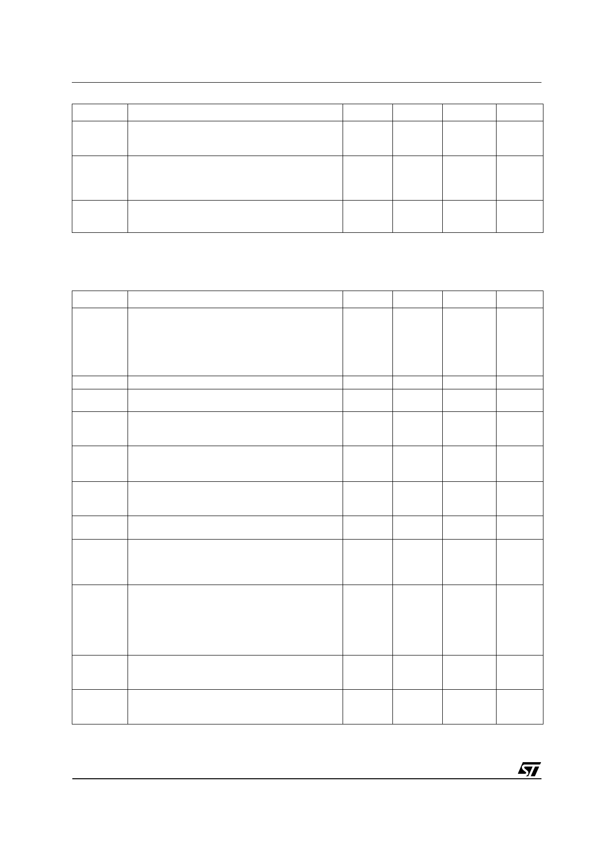
ELECTRICAL CHARACTERISTICS
Symbol
GBP
THD
en
Parameter
Gain Bandwidth Product
VCC = 30V,RL = 2k, CL = 100pF
f = 100kHz, Vin = 10mV
Total Harmonic Distortion
f = 1kHz
AV = 20dB,RL = 2k, VCC = 30V
CL = 100pF, Vo = 2Vpp
Equivalent Input Noise Voltage
f = 1kHz, Rs = 100Ω
Vcc = 30V
Min.
0.5
Typ.
0.9
0.02
Max.
Unit
MHz
%
50
nV/√Hz
1) The input common-mode voltage of either input signal voltage should not be allowed to go negative by more than 0.3V. The upper end
of the common-mode voltage range is VCC+ - 1.5V. Both inputs can go to Vcc+ 0.3V without damage.
OPERATOR 1 (op-amp with non-inverting input connected to the internal Vref)
VCC+ = +5V, VCC- = Ground, Tamb = 25°C (unless otherwise specified)
Symbol
Vio
DVio
Iib
Avd
SVR
Isource
Io
Isink
VOH
VOL
SR
Parameter
Input Offset Voltage
Vicm = 0V
TSM103WA, Tamb = 25°
Tmin. ≤ Tamb ≤ Tmax.
TSM103W, Tamb = 25°
Tmin. ≤ Tamb ≤ Tmax.
Input Offset Voltage Drift
Input Bias Current
negative input
Large Signal Voltage Gain
VCC = 15V, RL = 2k, Vo = 1.4V to 11.4V
Tmin. ≤ Tamb ≤ Tmax
Supply Voltage Rejection Ratio
Vicm = 0V
VCC+ = 5V to 30V
Output Current Source
Vo = 2V
VCC = +15V, Vid = +1V
Short Circuit to Ground
VCC = +15V
Output Current Sink
Vid = -1V,
VCC = +15V, Vo = 2V
VCC = +15V, Vo = 0.2V
High Level Output Voltage
VCC+ = 30V
Tamb = 25°C, RL = 2k
Tmin. ≤ Tamb ≤ Tmax.
Tamb = 25°C, RL = 10k
Tmin. ≤ Tamb ≤ Tmax.
Low Level Output Voltage
RL = 10k
Tmin. ≤ Tamb ≤ Tmax.
Slew Rate at Unity Gain
Vi = 0.5 to 2V, VCC = 15V
RL = 2k, CL = 100pF, unity gain
Min.
65
20
10
12
26
26
27
27
0.2
Typ.
0.5
1
7
20
100
100
40
40
20
50
27
28
5
0.4
Max.
Unit
2
3
4
mV
5
µV/°C
nA
V/mV
dB
mA
60
mA
mA
µA
V
20
20
mV
V/µs
4/7
Share Link: 