AD637 Просмотр технического описания (PDF) - Analog Devices
Номер в каталоге
Компоненты Описание
производитель
AD637 Datasheet PDF : 10 Pages
| |||
AD637
OPTIONAL TRIMS FOR HIGH ACCURACY
The AD637 includes provisions to allow the user to trim out
both output offset and scale factor errors. These trims will result
in significant reduction in the maximum total error as shown in
Figure 4. This remaining error is due to a nontrimmable input
offset in the absolute value circuit and the irreducible non-
linearity of the device.
The trimming procedure on the AD637 is as follows:
l. Ground the input signal, VIN and adjust R1 to give 0 V out-
put from Pin 9. Alternatively R1 can be adjusted to give the
correct output with the lowest expected value of VIN.
2. Connect the desired full scale input to VIN, using either a dc
or a calibrated ac signal, trim R3 to give the correct output at
Pin 9, i.e., 1 V dc should give l.000 V dc output. Of course, a
2 V peak-to-peak sine wave should give 0.707 V dc output.
Remaining errors are due to the nonlinearity.
5.0
AD637K MAX
2.5
INTERNAL TRIM
0
AD637K
EXTERNAL TRIM
2.5
AD637K: 0.5mV ؎0.2%
0.25mV ؎0.05%
EXTERNAL
5.0
0
0.5
1.0
1.5
2.0
INPUT LEVEL – Volts
Figure 4. Max Total Error vs. Input Level AD637K
Internal and External Trims
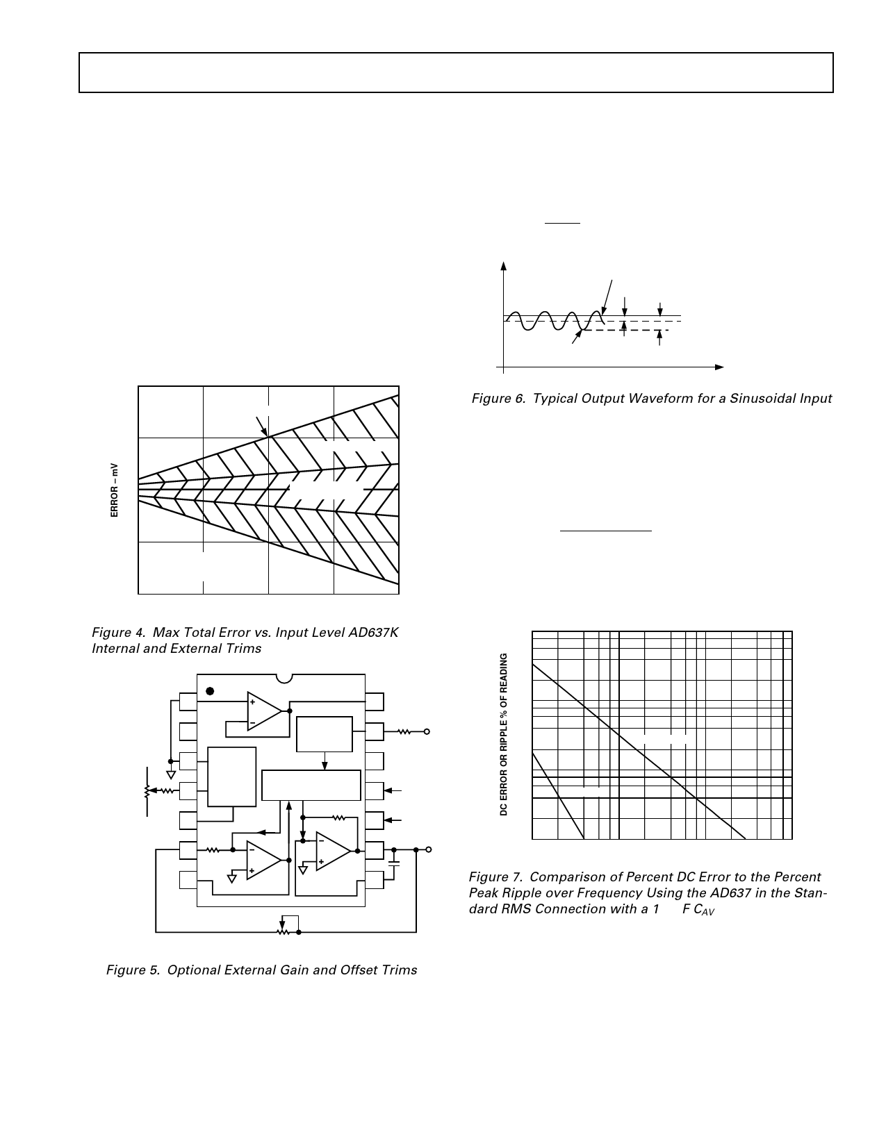
functions of input signal frequency f, and the averaging time
constant τ (τ: 25 ms/µF of averaging capacitance). As shown in
Figure 6, the averaging error is defined as the peak value of the
ac component, ripple, plus the value of the dc error.
The peak value of the ac ripple component of the averaging er-
ror is defined approximately by the relationship:
50
6.3 τf in % of reading where (t > 1/f)
EO
IDEAL
EO
DC ERROR = AVERAGE OF OUTPUT–IDEAL
AVERAGE ERROR
DOUBLE-FREQUENCY
RIPPLE
TIME
Figure 6. Typical Output Waveform for a Sinusoidal Input
This ripple can add a significant amount of uncertainty to the
accuracy of the measurement being made. The uncertainty can
be significantly reduced through the use of a post filtering net-
work or by increasing the value of the averaging capacitor.
The dc error appears as a frequency dependent offset at the
output of the AD637 and follows the equation:
1
0.16 + 6.4τ2 f 2 in % of reading
Since the averaging time constant, set by CAV, directly sets the
time that the rms converter “holds” the input signal during
computation, the magnitude of the dc error is determined only
by CAV and will not be affected by post filtering.
100
BUFFER
1
AD637
2
+VS
3
OUTPUT R1
OFFSET
ADJUST
50k⍀
4
R2
1M⍀
–VS
5
6
BIAS
SECTION
25k⍀
ABSOLUTE
VALUE
SQUARER/DIVIDER
25k⍀
7
FILTER
14
R4
147⍀
13
VIN
12
11
+VS
10
–VS
9
+
V rms
OUT
8
CAV
R3
1k⍀
SCALE FACTOR ADJUST,
؎2%
Figure 5. Optional External Gain and Offset Trims
CHOOSING THE AVERAGING TIME CONSTANT
The AD637 will compute the true rms value of both dc and ac
input signals. At dc the output will track the absolute value of
the input exactly; with ac signals the AD637’s output will ap-
proach the true rms value of the input. The deviation from the
ideal rms value is due to an averaging error. The averaging error
is comprised of an ac and dc component. Both components are
10
PEAK RIPPLE
1.0
DC ERROR
0.1
10
100
1k
10k
SINEWAVE INPUT FREQUENCY – Hz
Figure 7. Comparison of Percent DC Error to the Percent
Peak Ripple over Frequency Using the AD637 in the Stan-
dard RMS Connection with a 1 × µF CAV
The ac ripple component of averaging error can be greatly
reduced by increasing the value of the averaging capacitor.
There are two major disadvantages to this: first, the value of the
averaging capacitor will become extremely large and second, the
settling time of the AD637 increases in direct proportion to the
value of the averaging capacitor (Ts = 115 ms/µF of averaging
capacitance). A preferable method of reducing the ripple is
through the use of the post filter network, shown in Figure 8.
This network can be used in either a one or two pole configura-
tion. For most applications the single pole filter will give the
best overall compromise between ripple and settling time.
REV. E
–5–
Share Link: 