TP5322N8 Просмотр технического описания (PDF) - Supertex Inc
Номер в каталоге
Компоненты Описание
производитель
TP5322N8 Datasheet PDF : 2 Pages
| |||
TP5322
Thermal Characteristics
Package
TO-243AA
ID (continuous)
-0.26A
ID (pulsed)
-0.90A
Power Dissipation @
TA = 25°C
1.6W
θJC
°C/W
15
TO-236AB
-0.12A
-0.70A
0.36W
200
*ID(continous) is limited by max rated Tj.
**Mounted on FR4 board, 25mm x 25mm x 1.57mm. Significant PD increase possible on ceramic substate.
θJA
°C/W
78**
350
IDR*
-0.26A
-0.12A
IDRM
-0.9A
-0.7A
Electrical Characteristics (@25°C unless otherwise specified)
Symbol Parameter
Min Typ
BVDSS Drain-to-Source
Breakdown Voltage
-220
VGS(th) Gate Threshold Voltage
-1.0
∆VGS(th) Change in VGS(th) with Temperature
IGSS Gate Body Leakage
IDSS Zero Gate Voltage Drain Current
Max
-2.4
4.5
-100
-10
-1.0
Units
V
V
mV/°C
nA
µA
mA
ID(ON)
RDS(ON)
On-State Drain Current
Static Drain-to-Source
ON-State Resistance
-0.7 -0.95
A
10
15
Ω
8.0 12
∆RDS(ON) Change in RDS(ON) with Temperature
1.7 %/°C
GFS Forward Transconductance
100 250
mmho
CISS
COSS
Input Capacitance
Common Source Output Capacitance
110
45
pF
CRSS
td(ON)
tr
td(OFF)
tf
VSD
trr
Notes:
Reverse Transfer Capacitance
Turn-ON Delay Time
Rise Time
Turn-Off Delay Time
Fall Time
Diode Forward Voltage Drop
Reverse Recovery Time
20
10
15
ns
20
15
-1.8
V
300
ns
1) All DC parameters 100% tested at 25°C unless otherwise stated. (Pulsed test: 300µs pulse at 2% duty cycle.)
2) All AC parameters sample tested.
Conditions
VGS = 0V, ID = -2mA
VGS = VDS, ID = -1mA
VGS = VDS, ID = -1mA
VGS = ±20V, VDS = 0V
VGS = 0V, VDS = Max Rating
VGS = 0V, VDS = 0.8 Max
Rating, TA = 125°C
VGS = -10V, VDS = -25V
VGS = -4.5V, ID = -100mA
VGS = -10V, ID = -200mA
VGS = -10V, ID = -200mA
VDS = -25V, ID = -200mA
VGS = 0V, VDS = -25V
f = 1MHz
VDD = -25V,
ID = -0.7A
RGEN = 25 Ω
VGS = 0V, ISD = -0.5A
VGS = 0V, ISD = -0.5A
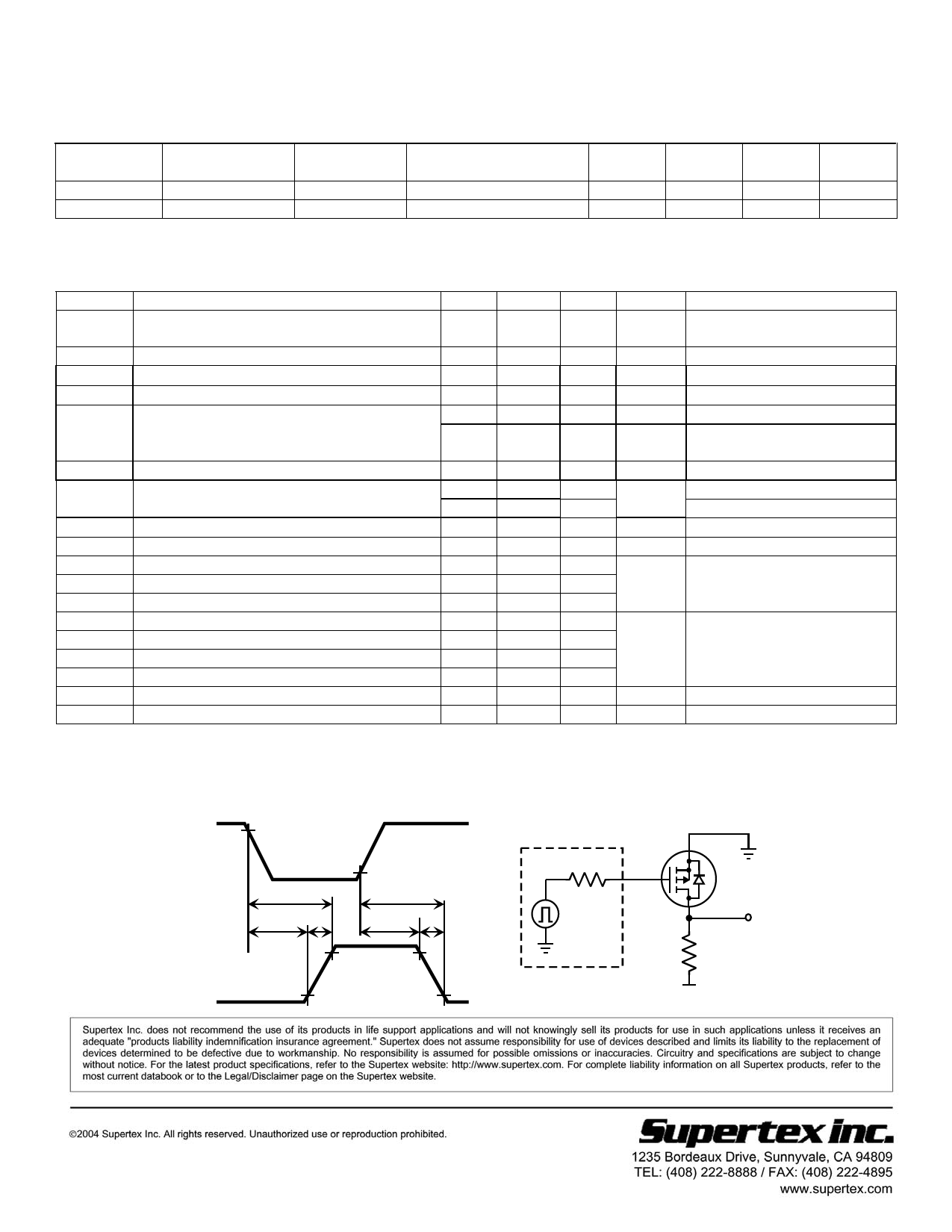
Switching Waveforms and Test Circuit
0V
Input
-10V
0V
Output
t(ON)
td(ON)
tr
t(OFF)
td(OFF) tf
VDD
Pulse
Generator
RGEN
Input
D.U.T
OUT PUT
RL
VDD
Doc.# DSFP-TP5322
A042005
2
Rev. 3 September 14, 2004
Share Link: 