TMC2246AG1C Просмотр технического описания (PDF) - Cadeka Microcircuits LLC.
Номер в каталоге
Компоненты Описание
производитель
TMC2246AG1C Datasheet PDF : 18 Pages
| |||
TMC2246A
PRODUCT SPECIFICATION
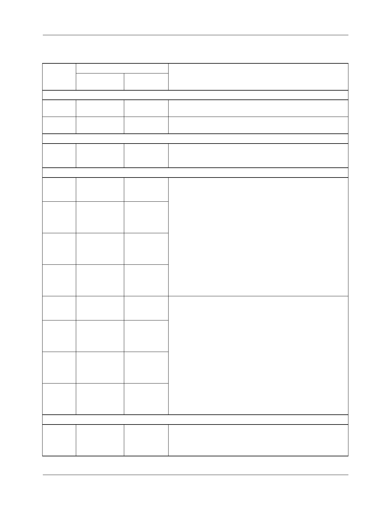
Pin Descriptions
Pin Name
Pin Number
CPGA/PPGA/
MPGA
MQFP
Pin Function Description
Power
VDD
F3, H3, L7, C8 12, 20, 46, 102 Supply Voltage. The TMC2246A operates from a single +5V
supply. All power and ground pins must be connected.
GND
E3, G3, J3, L6, 8, 16, 24, 42, Ground. The TMC2246A operates from a single +5V supply. All
H11, C7
72, 106
power and ground pins must be connected.
Clock
CLK
C3
1
System Clock. The TMC2246A operates from a single master
clock input. The rising edge of clock strobes all enabled registers.
All timing specifications are referenced to the rising edge of CLK.
Inputs
D19-0
M1, K3, L2, N1, 27, 28, 29, 30, Data Input Ports. D1 through D4 are the 10-bit data input ports.
L3, M2, N2, L4, 31, 32, 33, 34, The LSB is Dx0.
M3, N3
35, 36
D29-0
J12, K13, J11,
K12, L13, L12,
K11, M13, M12,
L11
70, 69, 68, 67,
66, 65, 64, 63,
62, 61
D39-0
J13, H12, H13,
G12, G11, G13,
F13, F12, F11,
E13
71, 73, 74, 75,
76, 77, 78, 79,
80, 81
D49-0
B4, C5, A4, B5,
A5, C6, B6, A6,
A7, B7
115, 114, 113,
112, 111, 110,
109, 108, 107,
105
C110-0
M4, L5, N4, M5, 37, 38, 39, 40, Coefficient Input Ports. C1 through C4 are the 11-bit coefficient
N5, M6, N6, M7, 41, 43, 44, 45, input ports. The LSB is Cx0.
N7, N8, M8
47, 48, 49
C210-0
N13, M11, L10,
N12, N11, M10,
L9, N10, M9,
N9, L8
60, 59, 58, 57,
56, 55, 54, 53,
52, 51, 50
C310-0
E12, D13, E11,
D12, C13, B13,
D11, C12, A13,
C11, B12
82, 83, 84, 85,
86, 87, 88, 89,
90, 91, 92
C410-0
A8, B8, A9, B9, 104, 103, 101,
A10, C9, B10, 100, 99, 98, 97,
A11, B11, C10, 96, 95, 94, 93
A12
Outputs
S15-0
C1, D2, D1, E2,
E1, F2, F1, G2,
G1, H1, H2, J1,
J2, K1, K2, L1
6, 7, 9, 10, 11,
13, 14, 15, 17,
18, 19, 21, 22,
23, 25, 26
Sum Output. The current 16-bit result is available at the Sum
output. The LSB is S0. See the Functional Block Diagram.
REV. 1.0.3 9/11/00
5
Share Link: 