TMC2072KHC Просмотр технического описания (PDF) - Fairchild Semiconductor
Номер в каталоге
Компоненты Описание
производитель
TMC2072KHC Datasheet PDF : 21 Pages
| |||
PRODUCT SPECIFICATION
TMC2072
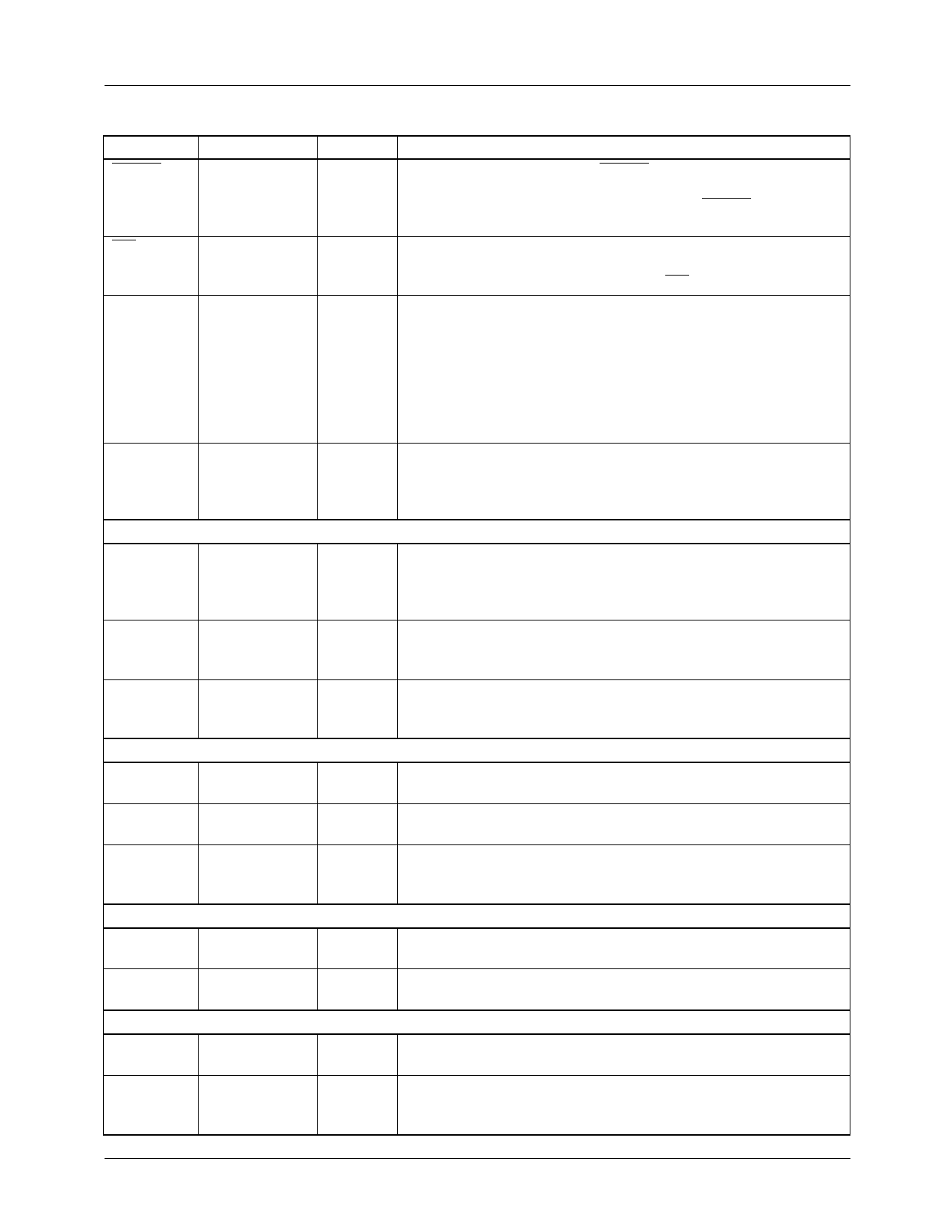
Pin Definitions (continued)
Pin Name
RESET
Pin Number
7
Pin Type
TTL
INT
VALID
17
TTL
34
TTL
BURL
31
Analog Interface
VREF
70
TTL/
CMOS
+1.23 V
COMP
88
0.1 µF
RB, RT
57, 68
0.1 µF
PLL Filter
DDS OUT
82
PFD IN
77
CBYP
75
1 µF
Power Supply
VDDA
49, 51, 52, 60,
64, 73, 87
VDD
6, 18, 26, 42, 44,
48, 92, 98, 100
Ground
AGND
50, 55, 63, 67,
69, 72, 74, 81, 89
DGND
8, 16, 27, 38, 39,
41, 46, 47, 90,
95-97
+5 V
+5 V
0.0 V
0.0 V
Function
Master reset input. Bringing RESET LOW forces the internal state
machines to their starting states, loads the Control Register with
default values, and disables outputs. Bringing RESET HIGH restarts
the TMC2072 in its default mode.
Interrupt output. This output is LOW if the internal horizontal phase
lock loop is unlocked with respect to incoming video for 128 or more
lines per field. After lock is established, INT goes HIGH.
HSYNC locked flag. Hsync locked flag. When high, this output
indicates that the most recent incoming horizontal sync has been
detected within ±16 pixels of its expected position. It goes low if no
sync is encountered during this ±16-pixel window, as during a
typical VCR headswitch line. Once the chip has locked to a clean
video source, this flag should remain high continuously. If the chip
has locked to a VCR, this flag will typically go low for one (or
sometimes two) lines at the bottom of each field.
Burst lock flag. When high, this output indicates that the chip’s
internal subcarrier synthesizer is phase-aligned with the current
line’s incoming chroma burst. The flag goes low when the internal
and external phases diverge.
VREF input/output. +1.23 Volt reference. When the internal voltage
reference is used, this pin should be decoupled to AGND with a 0.1
µF capacitor. An external +1.2 Volt reference may be connected
here, overriding the internal reference source.
Compensation capacitor. Compensation for DDS D/A converter
circuitry. This pin should be decoupled to VDDA with a 0.1 µF
capacitor.
A/D VREF decoupling. Decoupling points for A/D converter voltage
references. These pins should be decoupled to AGND with a 0.1 µF
capacitor.
Internal DDS output. Analog output from the internal Direct Digital
Synthesizer D/A converter, at 1/9 the PXCK frequency.
Horizontal PLL input. Analog input to the Phase/Frequency
Detector of the horizontal phase-locked loop.
Comparator bypass. Decoupling point for the internal comparator
reference of the Phase/Frequency Detector. This pin should be
decoupled to AGND with a 0.1 µF capacitor.
Analog power supply. Positive power supply to analog section.
All pins must be connected.
Digital power supply. Positive power supply to digital section.
All pins must be connected.
Analog ground. Ground for analog section. All pins must be
connected.
Digital ground. Ground for digital section. All pins must be
connected.
REV. 1.0.4 6/19/01
7
Share Link: 