TMC2072 Просмотр технического описания (PDF) - Fairchild Semiconductor
Номер в каталоге
Компоненты Описание
производитель
TMC2072 Datasheet PDF : 21 Pages
| |||
TMC2072
PRODUCT SPECIFICATION
Details (continued)
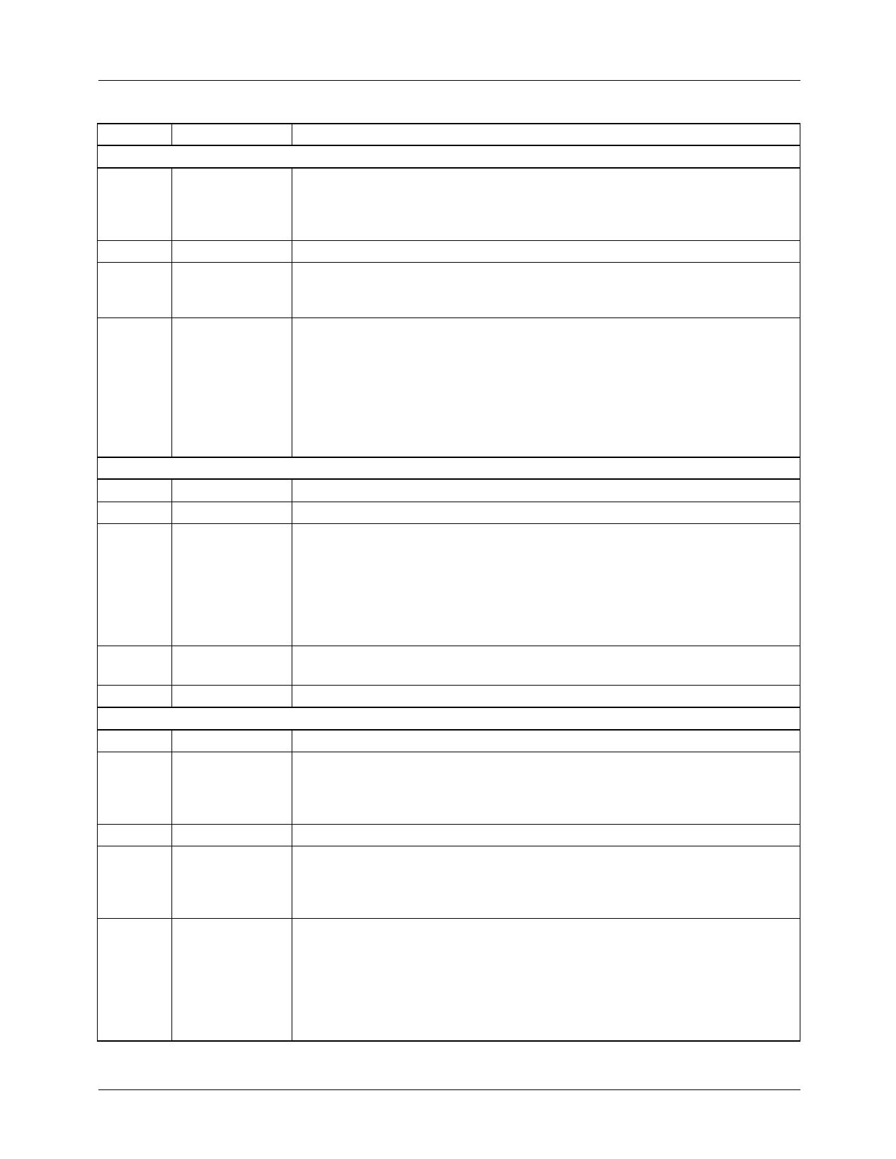
Bit
Name
Function
Reg 0A Gain, loop filter, subpixel adjust
7
V_GAIN
Analog Gain into A/D Converter. LOW (power-on default): unity gain, suitable
for nominal 1-volt (sync tip to reference white) video signals. HIGH: 1.5 X gain, for
over-terminated video signals with approximately 200mV sync tips. [TMC22071A
bit 9.]
6
DDS_TEST
Reserved, test bit for DDSDAC; reset low (power-on default)
5
HFILT
Horizontal Phase-Locked Loop Filter Bandwidth. LOW (power-on default):
narrow H loop filter to minimize jitter with clean video sources. HIGH: wide filter
bandwidth, to better accommodate jittery or noisy sources.
4:0
SUBPIX
Sample Clock (and Sync Signal) Subpixel Offset Timing Control. Format is
fractional two’s complement, i.e., 0.SFFFF, where bit 4, the signed most
significant bit (S), represents 1 PXCK or 1/2 pixel. Thus, the programming range
is 01111 = +15/32 pixel to 10000 = -16/32 pixel. A value of 01000 will advance the
sample clock and syncs by 1/4 pixel relative to the incoming video, whereas a
value of 11000 will retard them the same amount. The power-on default value of
0 nominally aligns the sample clock with the center of the incoming signal’s falling
sync edges. [TMC22071A bits 16:12.]
Reg 0B Input select
7
Reserved, reset low (power-on default)
6
NCOMP
Reserved, test bit: noise comparator disable; reset low (power-on default)
5:4
SOURCE
These two bits determine which of the three analog input lines is active, as
follows:
00 VIN1 (power-on default)
01 VIN2
1X VIN3.
[TMC22071A bits 8:7.]
3
SCALE
Reset low (power-on default) to compensate burst PLL for line-by-line changes in
sampling rate. Set high to disable compensation (test purpose only).
2:0
ANTEST
Reserved, analog circuit test bits; reset low (power-on default)
Reg 0C Field and Vsync reporting
7
Reserved, reset low (power-on default)
6
FID FREE
LOW (power-on default): The color frame identifier (FID[1] in NTSC) toggles
smoothly, but with no guaranteed relationship to the incoming color burst phase.
HIGH freezes FID[1] in NTSC mode, if a two-field (odd/even only) sequence is
desired.
5:3
Reserved, reset low (power-on default)
2
DLYRPTF
Delay Field i.d. Update. LOW (power-on default): FID will increment at the start
of each incoming vertical sync pulse group. (NTSC lines 4 and 266.) HIGH: FID
will increment at the start of the next line after the start each incoming vertical
sync.
1
DLYRPT
Delay GVSYNC Output. LOW (power-on default): TMC2072 will generate a
GVSYNC falling edge as it predicts the start of a new vertical sync series. This is
recommended for laser disk or higher quality video signals, for which the chip can
easily predict video field timing. HIGH: TMC2072 will generate a GVSYNC falling
edge on the line after it detects the start of a vertical sync series. This is
recommended for jittery input signals, if a one-line upward image displacement is
acceptable.
10
REV. 1.0.4 6/19/01
Share Link: 