74VHC4046CW Просмотр технического описания (PDF) - Fairchild Semiconductor
Номер в каталоге
Компоненты Описание
производитель
74VHC4046CW Datasheet PDF : 16 Pages
| |||
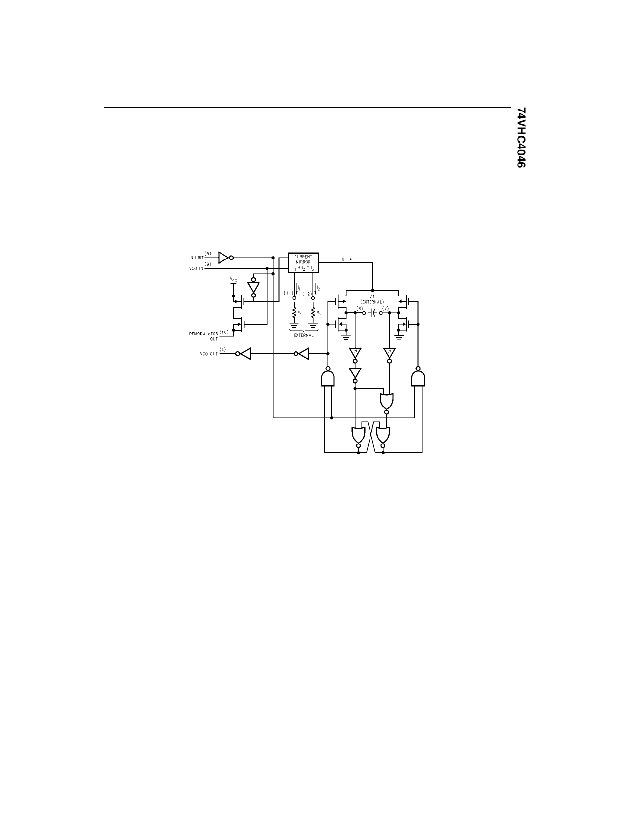
Detailed Circuit Description
VOLTAGE CONTROLLED OSCILLATOR/SOURCE
FOLLOWER
The VCO requires two or three external components to
operate. These are R1, R2, C1. Resistor R1 and capacitor
C1 are selected to determine the center frequency of the
VCO. R1 controls the lock range. As R1’s resistance
decreases the range of fMIN to fMAX increases. Thus the
VCO’s gain increases. As C1 is changed the offset (if used)
of R2, and the center frequency is changed. (See typical
performance curves) R2 can be used to set the offset fre-
quency with 0V at VCO input. If R2 is omitted the VCO
range is from 0Hz. As R2 is decreased the offset frequency
is increased. The effect of R2 is shown in the design infor-
mation table and typical performance curves. By increasing
the value of R2 the lock range of the PLL is offset above
0Hz and the gain (Hz/Volt) does not change. In general,
when offset is desired, R2 and C1 should be chosen first,
and then R1 should be chosen to obtain the proper center
frequency.
FIGURE 1. Logic Diagram for VCO
Internally the resistors set a current in a current mirror as
shown in Figure 1. The mirrored current drives one side of
the capacitor once the capacitor charges up to the thresh-
old of the Schmitt Trigger the oscillator logic flips the
capacitor over and causes the mirror to charge the oppo-
site side of the capacitor. The output from the internal logic
is then taken to pin 4.
The input to the VCO is a very high impedance CMOS
input and so it will not load down the loop filter, easing the
filters design. In order to make signals at the VCO input
accessible without degrading the loop performance a
source follower transistor is provided. This transistor can
be used by connecting a resistor to ground and its drain
output will follow the VCO input signal.
An inhibit signal is provided to allow disabling of the VCO
and the source follower. This is useful if the internal VCO is
not being used. A logic high on inhibit disables the VCO
and source follower.
The output of the VCO is a standard high speed CMOS
output with an equivalent LSTTL fanout of 10. The VCO
output is approximately a square wave. This output can
either directly feed the comparator input of the phase com-
parators or feed external prescalers (counters) to enable
frequency synthesis.
PHASE COMPARATORS
All three phase comparators share two inputs, Signal In
and Comparator In. The Signal In has a special DC bias
network that enables AC coupling of input signals. If the
signals are not AC coupled then this input requires logic
levels the same as standard 74VHC. The Comparator input
is a standard digital input. Both input structures are shown
in Figure 2.
The outputs of these comparators are essentially standard
74VHC voltage outputs. (Comparator II is 3-STATE.)
9
www.fairchildsemi.com
Share Link: 