HT23C512(1998) –ü—Ä–æ—Å–º–æ—Ç—Ä —Ç–µ—Ö–Ω–∏—á–µ—Å–∫–æ–≥–æ –æ–ø–∏—Å–∞–Ω–∏—è (PDF) - Holtek Semiconductor
–ù–æ–º–µ—Ä –≤ –∫–∞—Ç–∞–ª–æ–≥–µ
–ö–æ–º–ø–æ–Ω–µ–Ω—Ç—ã –û–ø–∏—Å–∞–Ω–∏–µ
–ø—Ä–æ–∏–∑–≤–æ–¥–∏—Ç–µ–ª—å
HT23C512 Datasheet PDF : 8 Pages
| |||
HT23C512
Symbol
Parameter
VIH
VOL
VOH
ILI
ILO
ISTB1
Input High Voltage
Output Low Voltage
Output High Voltage
Input Leakage Current
Output Leakage Current
Standby Current
ISTB2
CIN
COUT
Standby Current
Input Capacitance (See note)
Output Capacitance (See note)
Test Conditions
VCC Conditions
5V
—
5V IOL=3.2mA
5V IOH= –1mA
5V VIN=0 to VCC
5V VOUT=0 to VCC
5V
CE=VIL
CE=VIH
5V
CE ≤0.2V
CE ‚â•VCC-0.2V
— f=1MHz
— f=1MHz
Min. Typ. Max. Unit
2.2 — VCC V
— — 0.4 V
2.4 — VCC V
—
—
10 µA
—
—
10 µA
— — 1.5 mA
—
—
30 µA
— — 10 pF
— — 10 pF
Note: These parameters are periodically sampled but not 100% tested.
A.C. Characteristics
Ta=–40°C to 85°C
Symbol
Parameter
tCYC
tAA
tACE
tAOE
tOH
tOD
tOE
Cycle Time
Address Access Time
Chip Enable Access Time
Output Enable Access Time
Output Hold Time
Output Disable Time (See Note)
Output Enable Time (See Note)
VCC=2.7V~3.6V
Min. Max.
250
—
—
250
—
250
—
150
—
—
—
—
—
—
VCC=4.5V~5.5V
Min. Max.
150
—
—
150
—
150
—
80
10
—
—
70
10
—
Unit
ns
ns
ns
ns
ns
ns
ns
Note: These parameters are periodically sampled but not 100% tested.
A.C. test conditions
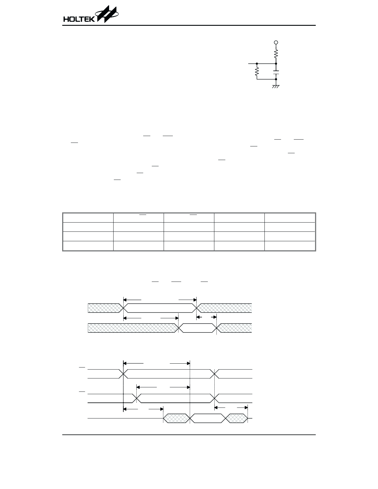
Output load: see figure right
Input rise and fall time: 10ns
Input pulse levels: 0.4V to 2.4V
Input and output timing reference levels:
0.8V and 2.0V (VCC=5V)
1.5V (VCC=3V)
Output load circuit
4
24th Aug ’98
Share Link: 