TDA9901TS Просмотр технического описания (PDF) - Philips Electronics
Номер в каталоге
Компоненты Описание
производитель
TDA9901TS Datasheet PDF : 20 Pages
| |||
Philips Semiconductors
Wideband differential digital controlled
variable gain amplifier
Product specification
TDA9901
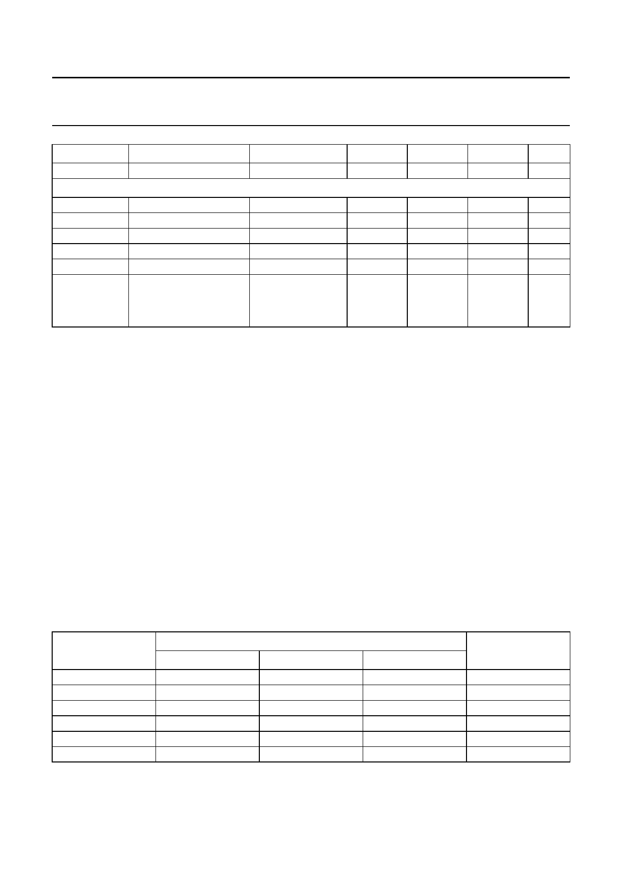
SYMBOL
PARAMETER
CONDITIONS
MIN.
TYP.
MAX.
UNIT
Ci
input capacitance
−
−
Clock inputs in differential mode
VIL
LOW-level input voltage VDDA = 5.0 V; note 6 3.19
−
VIH
HIGH-level input voltage VDDA = 5.0 V; note 6 3.83
−
IIH
HIGH-level input current
15
−
IIL
LOW-level input current
−40
−
Ci
input capacitance
−
−
∆Vi(CLK )(p-p)
differential AC input
DC voltage
0.1
−
voltage for switching
level = 2.5 V
CLK or CLKN
(peak-to-peak value)
2
pF
3.52
V
4.12
V
80
µA
−5
µA
2
pF
2.0
V
Notes
1. Due to on-chip regulator behaviour a warm-up time of 1 minute (typical) is recommended for optimal performance.
2. The analog output voltages are positive with respect to AGND.
3. In latching mode (TE = 0), the gain settling is latched at the rising edge of the clock input.
4. In transparent mode, the gain settling is directly controlled by the input data pattern.
5. The circuit may be used with a single TTL clock on CLK or CLKN. The non used clock pin has to be decoupled to
ground with a 100 nF capacitance.
6. There are four modes of operation for the clock inputs in non TTL mode:
a) PECL mode 1: (DC level vary 1 : 1 with VDDA) CLK and CLKN inputs are differential PECL levels.
b) PECL mode 2: (DC level vary 1 : 1 with VDDA) CLK input is at PECL level and gain change takes place on the
rising edge of the clock input signal when in latched mode. A DC level of 3.65 V has to be applied on CLKN
decoupled to VSSD via a 100 nF capacitor.
c) PECL mode 3: (DC level vary 1 : 1 with VDDA) CLKN input is at PECL level and gain change takes place on the
rising edge of the clock input signal when in latched mode. A DC level of 3.65 V has to be applied on CLK
decoupled to VSSD via a 100 nF capacitor.
d) AC driving mode 4: when driving the CLK input directly and with any AC signal of minimum 0.1 V (p-p) and with
a DC level of 2.5 V, the gain change takes place on the rising edge of the clock signal. When driving the CLKN
input with the same signal, gain change takes place on the falling edge of the clock signal. It is recommended to
decouple the CLKN or CLK input to VSSD via a 100 nF capacitor.
Table 1 Input coding
STATE
0
1
2
3
4
Other
GREY INPUT DATA CODE
D2
D1
D0
0
0
0
0
0
1
0
1
1
0
1
0
1
1
0
−
−
−
GAIN (dB)
minimum
minimum + 6
minimum + 12
minimum + 18
minimum + 24
minimum + 24
1999 Oct 08
9
Share Link: 