TDA3664 Просмотр технического описания (PDF) - NXP Semiconductors.
Номер в каталоге
Компоненты Описание
производитель
TDA3664 Datasheet PDF : 16 Pages
| |||
NXP Semiconductors
TDA3664
Very low dropout voltage/quiescent current 5 V voltage regulator
Remark: In the event of using different types of capacitors, a minimum ESR needs to
be created by using an additional resistor that is placed in series with the output
capacitor, see Figure 4.
• It is recommended not to use below 1 mA output current because of reduced phase
margin.
Table 8: Minimum ESR values required
IREG (mA) max C2 = 100 nF
1
>0Ω
C2 = 1 µF
> 1.5 Ω
5
>1Ω
> 0.5 Ω
10
>0Ω
> 0.5 Ω
100
>0Ω
> 0.5 Ω
C2 = 10 µF
> 2.5 Ω
>1Ω
>4Ω
>4Ω
C2 = 100 µF
>0Ω
>0Ω
>0Ω
>0Ω
11.3 Application circuits
The maximum output current of the regulator equals:
I REG(max) = -R---t--h---(--j--–---1-a--5)---0×-----–(---V-T---P-a---m–---b--V----R---E---G----) = 1----0-1--0-5---0×----–-(--V--T---P-a---m–---b-5----)(mA)
When Tamb = 21 °C, the maximum output current equals 140 mA at VP =14 V.
The total thermal resistance of the TDA3664 (SOT223-1 package) can be decreased to
lower values when pin 4 and body of the package are soldered to the printed-circuit board.
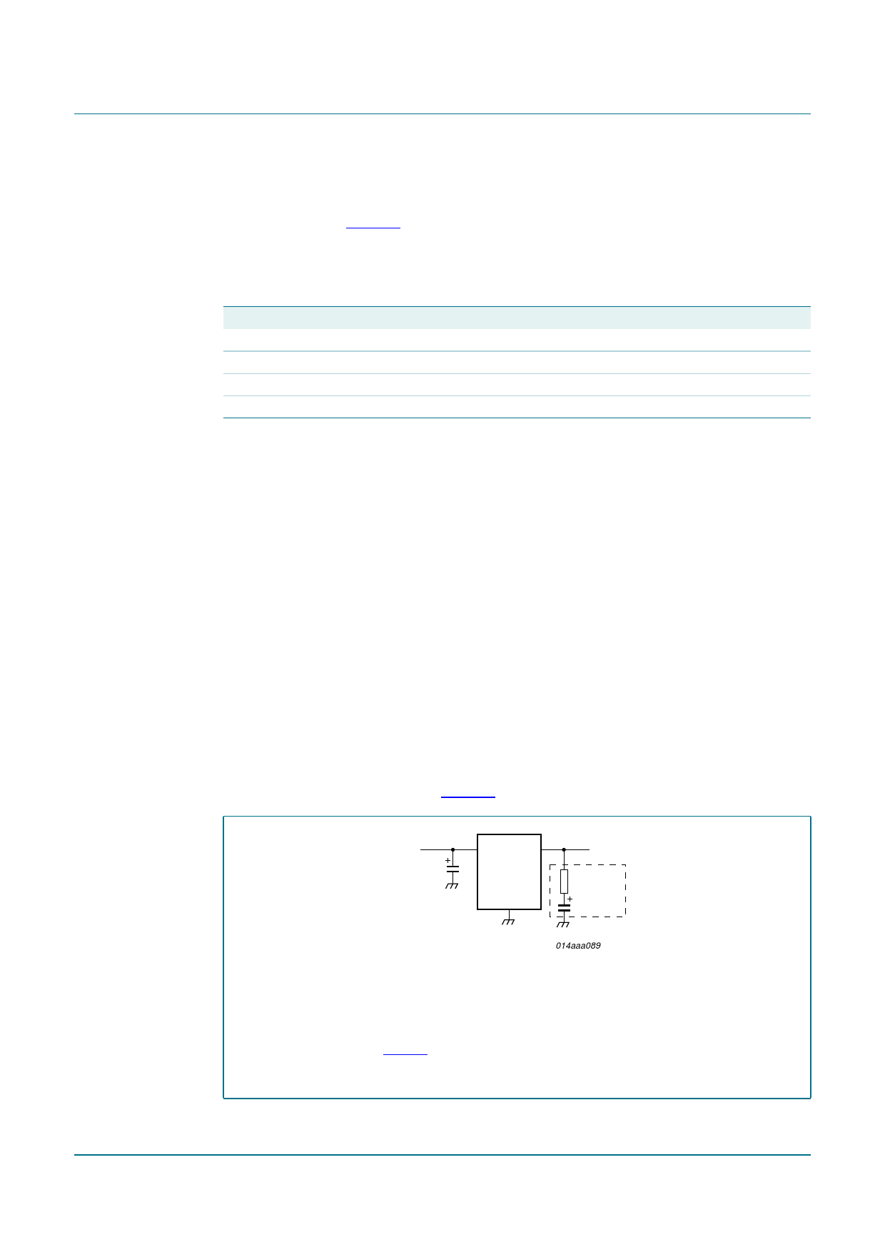
11.3.1 Application circuit with backup function
Sometimes, a backup function is needed to supply, for example, a microcontroller for a
short period of time when the supply voltage spikes to 0 V (or even −1 V).
This function can easily be built with the TDA3664 by using a large output capacitor. When
the supply voltage is 0 V (or −1 V), only a small current will flow into pin REG from this
large output capacitor (a few µA).
The application circuit is given in Figure 4.
VP
C1(1)
1 µF
1
3
TDA3664
2, 4
VREG(3)
C2(2)
014aaa089
(1) C1 is optional (to minimize supply noise only)
(2) C2 ≤ 4700 µF
(3) VREG = 5 V
(4) For reliable operation, it is recommended to have a minimum ESR of 3 Ω of the output
capacitor total (see Figure 4 above) and to have a stable application independent of load
current, temperature or output capacitance.
Fig 4. Application circuit with backup function (SO4 version)
TDA3664_7
Product data sheet
Rev. 07 — 25 June 2007
© NXP B.V. 2007. All rights reserved.
7 of 16
Share Link: 