TDA3617 Просмотр технического описания (PDF) - Philips Electronics
Номер в каталоге
Компоненты Описание
производитель
TDA3617 Datasheet PDF : 16 Pages
| |||
Philips Semiconductors
Multiple voltage regulator
Preliminary specification
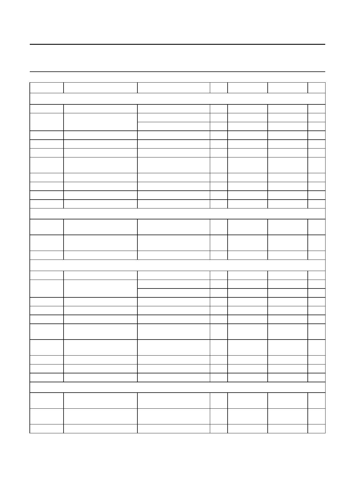
TDA3617
SYMBOL
PARAMETER
Regulator 1 (IREG1 = 5 mA)
VREG1(off)
VREG1
output voltage off
output voltage
∆VREG1
∆VREGL1
IqREG1
SVRR1
line regulation
load regulation
quiescent current
supply voltage ripple
rejection
VREG1d
IREG1m
IREG1sc
αct
drop-out voltage
current limit
short-circuit current
cross talk noise
Schmitt trigger for hold of regulator 1
Vthr
rising threshold voltage of
regulator 1
Vthf
falling threshold voltage of
regulator 1
Vhys
hysteresis voltage
Regulator 2 (IREG2 = 5 mA)
VREG2(off)
VREG2
output voltage off
output voltage
∆VREG2
∆VREGL2
IqREG2
SVRR2
VREG2d
line regulation
load regulation
quiescent current
supply voltage ripple
rejection
drop-out voltage
IREG2m
IREG2sc
αct
current limit
short-circuit current
cross talk noise
Schmitt trigger for hold of regulator 2
Vthr
rising threshold voltage of
regulator 2
Vthf
falling threshold voltage of
regulator 2
Vhys
hysteresis voltage
CONDITIONS
1 mA ≤ IREG1 ≤ 1.3 A
10.5 V ≤ VP ≤ 17.5 V
10.5 V ≤ VP ≤ 17.5 V
1 mA ≤ IREG1 ≤ 1.3 A
IREG1 = 1.3 A
f = 3 kHz; Vi(p-p) = 2 V
IREG1 = 1.3 A; note 3
VREG1 > 7.5 V; note 4
RL ≤ 0.5 Ω; note 5
note 6
VP rising
VP falling
0.5 mA ≤ IREG2 ≤ 600 mA
8 V ≤ VP ≤ 17.5 V
8 V ≤ VP ≤ 17.5 V
1 mA ≤ IREG2 ≤ 600 mA
IREG2 = 0.4 A
f = 3 kHz; Vi(p-p) = 2 V
IREG2 = 600 mA; VP = 6 V;
note 3
VREG2 > 4 V; note 4
RL ≤ 0.5 Ω; note 5
note 6
VP rising
VP falling
MIN.
TYP.
−
1
8.55 9.0
8.55 9.0
−
20
−
35
−
45
60 70
−
0.5
1.3 1.4
250 500
−
25
−
VREG1 − 0.15
8.1 VREG1 − 0.35
0.1 0.2
−
1
4.75 5.0
4.75 5.0
−
2
−
20
−
10
60 70
−
1
0.65 0.8
100 300
−
25
−
VREG1 − 0.15
4.3 VREG1 − 0.35
0.1 0.2
MAX.
UNIT
400
mV
9.45
V
9.45
V
50
mV
70
mV
110
mA
−
dB
1
V
−
A
−
mA
150
µV
VREG1 − 0.075 V
−
V
0.3
V
400
mV
5.25
V
5.25
V
50
mV
85
mV
40
mA
−
dB
1.5
V
−
A
−
mA
150
µV
VREG1 − 0.075 V
−
V
0.3
V
1999 Jul 14
7
Share Link: 