TDA1562Q Просмотр технического описания (PDF) - NXP Semiconductors.
Номер в каталоге
Компоненты Описание
производитель
TDA1562Q Datasheet PDF : 24 Pages
| |||
Philips Semiconductors
70 W high efficiency power amplifier
with diagnostic facility
Preliminary specification
TDA1562Q; TDA1562ST;
TDA1562SD
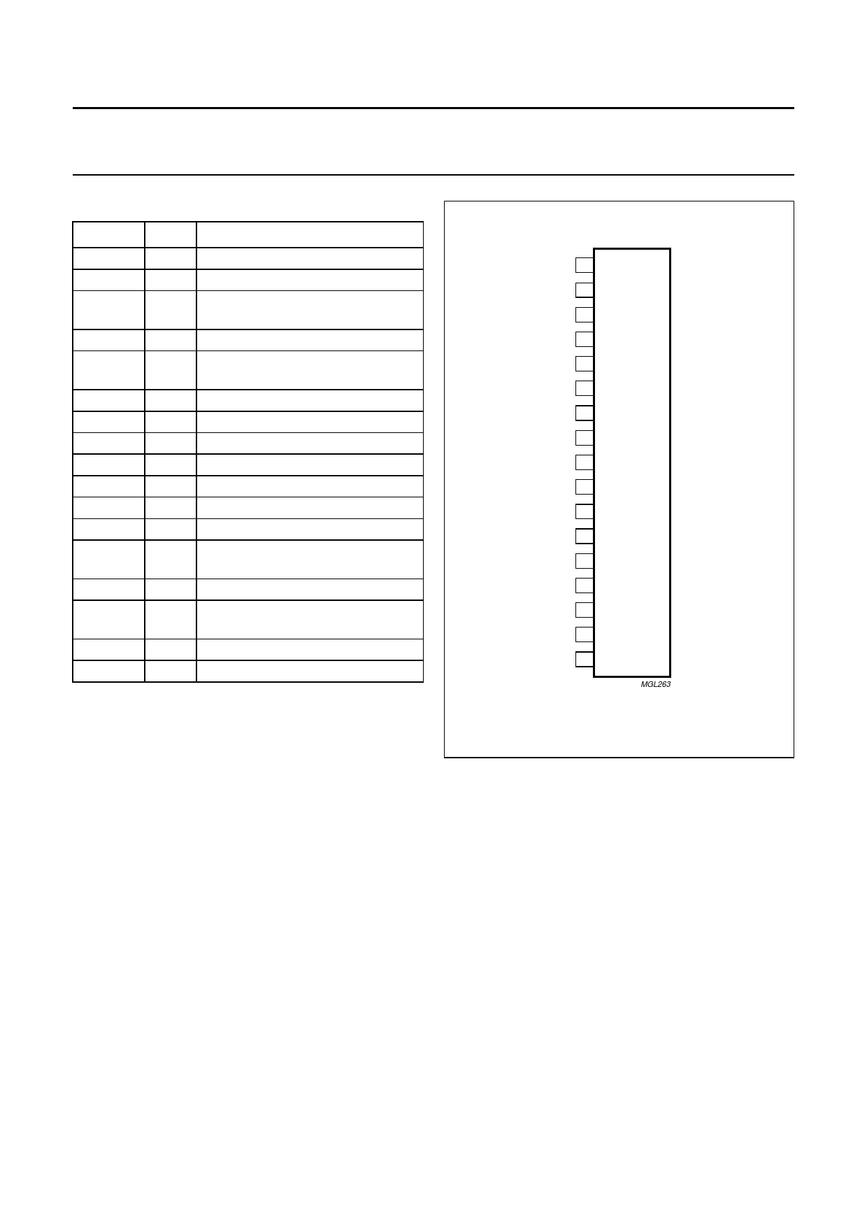
PINNING
SYMBOL PIN
DESCRIPTION
IN+
1 signal input (positive)
IN−
2 signal input (negative)
C1−
3 negative terminal of lift electrolytic
capacitor 1
MODE
4 mode select input
C1+
5 positive terminal of lift electrolytic
capacitor 1
PGND1
6 power ground 1
OUT+
7 positive output
DIAG
8 diagnostic output (open-collector)
VP1
VP2
OUT−
9 supply voltage 1
10 supply voltage 2
11 negative output
PGND2
12 power ground 2
C2+
13 positive terminal of lift electrolytic
capacitor 2
Vref
14 internal reference voltage
C2−
15 negative terminal of lift electrolytic
capacitor 2
STAT
16 status I/O
SGND
17 signal ground
handbook, halfpage
IN+ 1
IN− 2
C1− 3
MODE 4
C1+ 5
PGND1 6
OUT+ 7
DIAG 8
VP1 9 TDA1562Q
TDA1562ST
VP2 10 TDA1562SD
OUT− 11
PGND2 12
C2+ 13
Vref 14
C2− 15
STAT 16
SGND 17
MGL263
Fig.2 Pin configuration.
2003 Feb 12
5
Share Link: 