TDA10045 Просмотр технического описания (PDF) - Philips Electronics
Номер в каталоге
Компоненты Описание
производитель
TDA10045 Datasheet PDF : 16 Pages
| |||
Philips Semiconductors
Single Chip DVB-T Channel Receiver
Preliminary specification
TDA10045
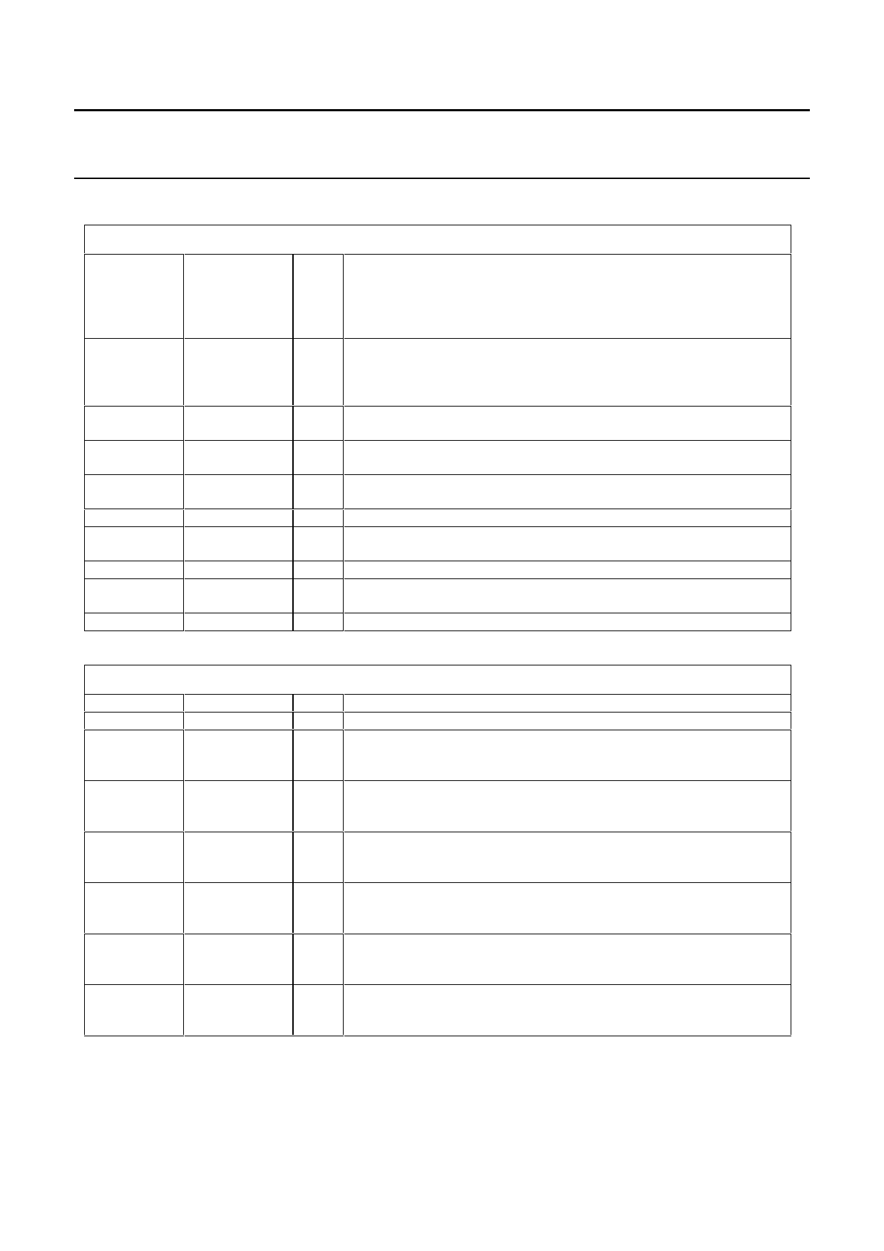
ON-CHIP ADC SIGNALS
92
VIM
I
VIP
VREFP
VREFM
VD1
VS1
VD2
VS2
VD3
VS3
91
I
94
O
93
O
100
I
99
I
98
I
97
I
95-90
I
96-89
I
Negative input to the A/D converter. This pin is DC biased to half
supply through an internal resistor divider (2x20K resistors). In order
to remain in the range of the ADC, the voltage difference between pins
VIP and VIM should be between -0.5 and 0.5 volts (See SW I2C
register).
Positive input to the A/D converter. This pin is DC biased to half supply
through an internal resistor divider (2x20K resistors). In order to
remain in the range of the ADC, the voltage difference between pins
VIP and VIM should be between –0.5 and 0.5 volts.
Positive voltage reference for the A/D converter. See SW I2C register
for the output level.
Negative voltage reference for the A/D converter. See SW I2C register
for the output level.
Power supply input for the digital switching circuitry sensitive to the
supply noise. The DC voltage should be 1,8V.
Ground return for the digital switching circuitry.
Power supply input for the analog clock drivers. The DC voltage should
be 3.3V.
Ground return for the analog clock drivers.
Power supply input for the analog circuits. The DC voltage should be
3.3V.
Ground return for analog circuits.
I2C INTERFACES
SCL
SDA
SADDR[1:0]
11
12
16-17
9
SCL_TUN
10
SDA_TUN
SCL_EEP
5
SDA_EEP
8
15
EEPADDR
I I2C master serial clock. Up to 700 kbit/s.
I/O I2C master serial data inout, open drain I/O pad.
SADDR[1:0] are the 2 LSBs of the I2C address of the TDA10045. The
I MSBs are internally set to 00010. Therefore the complete I2C address
of the TDA10045 is (MSB to LSB): 0,0,0,1,0,SADDR[1], SADDR[0]
Tuner I2C serial clock signal.This signal derived from the master SCL
OD can be set to high impedance when no tuner acces needed. (See
BP_I2C_TUN register) (open drain)
Tuner I2C serial data signal.This signal derived from the master SDA
I/O can be set to high impedance when no tuner acces needed. (See
BP_I2C_TUN register) (open drain)
O Extra I2C clock to download DSP code from an external EEPROM.
(Optional mode). Can be connected to the master I2C Bus. (open
drain)
I/O Extra I2C data bus to download DSP code from an external
EEPROM. (Optional mode). Can be connected to the master I2C Bus.
(open drain)
EEPRAD is the LSB of the I2C address of the EEPROM. The MSBs
I are internally set to 101000. Therefore the complete I2C address of
the EEPROM is (MSB to LSB): 1,0,1,0,0,0, EEPADDR
2000 March 15
5
Share Link: 