LC7470 Просмотр технического описания (PDF) - SANYO -> Panasonic
Номер в каталоге
Компоненты Описание
производитель
LC7470 Datasheet PDF : 13 Pages
| |||
LC7470
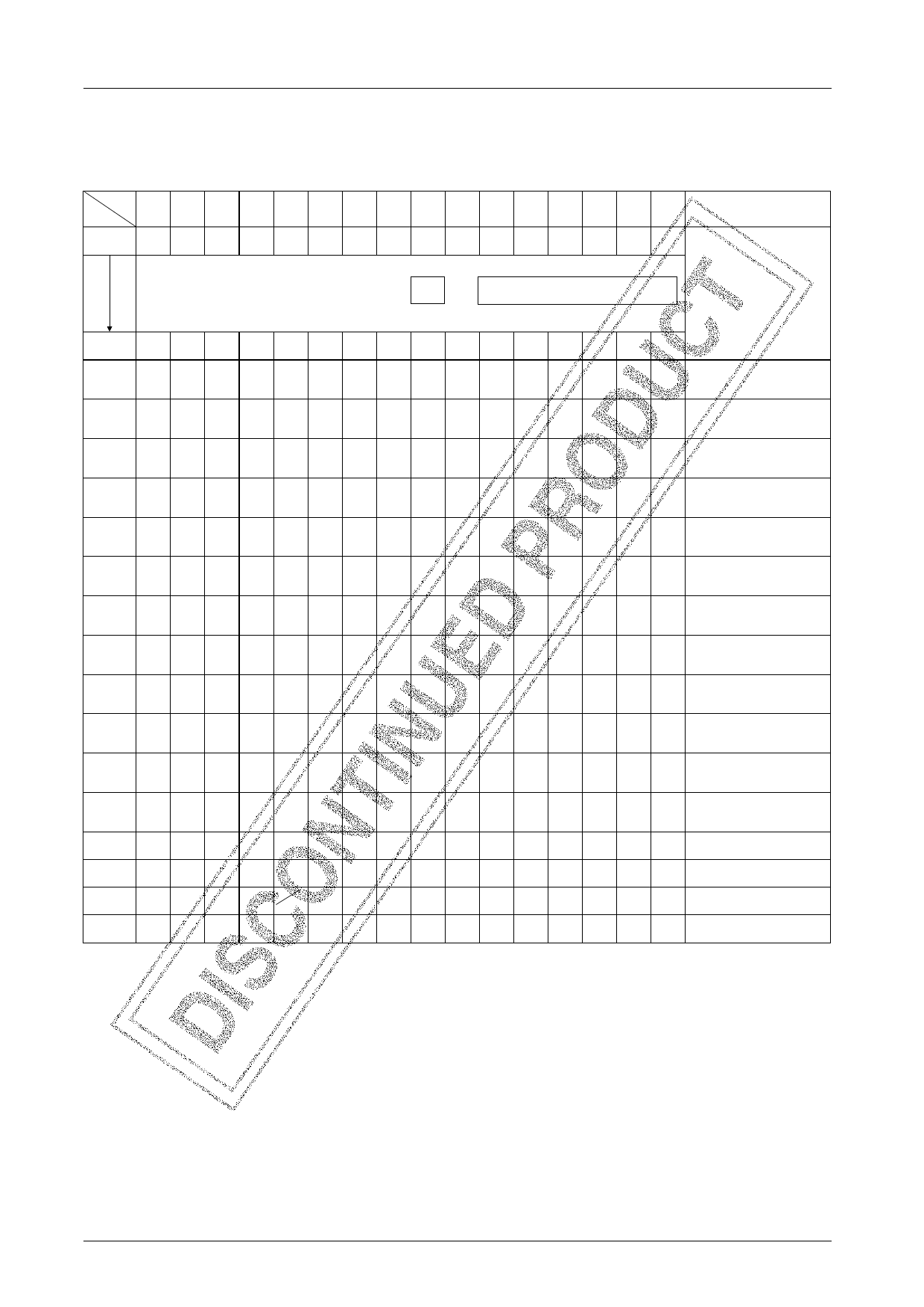
Memory Configuration (display RAM and control RAM)
Memory address and data signals consist of 16 bits.
Address range from 0D (000h) to 175D (0AFh) used as the display RAM.
Address range from 176D (0B0h) to 191D (0BFh) is used as the display control register data area.
Bit
Address
DA DA DA DA DA DA DA DA DA DA DA DA DA DA DA DA
F
E DC B A
9
8
7
6
5
4
3
2
10
000
(000h)
0
0
0
0
0
0
0
0 BLINK 0 C5 C4 C3 C2 C1 C0
Remarks
Blinking
Character code
Display RAM area
175
(0AFh)
0
0
0
0
0
0
0
0 BLINK 0 C5 C4 C3 C2 C1 C0
176
(0B0h)
0
0
0
0
Display line ROM
- ADRA ADR9 ADR8 ADR7 ADR6 ADR5 ADR4 ADR3 ADR2 ADR1 ADR0 specification. First character
of the first line
177
(0B1h)
0
0
0
0
Display line ROM
- ADRA ADR9 ADR8 ADR7 ADR6 ADR5 ADR4 ADR3 ADR2 ADR1 ADR0 specification. First character
of the second line
178
(0B2h)
0
0
0
0
Display line ROM
- ADRA ADR9 ADR8 ADR7 ADR6 ADR5 ADR4 ADR3 ADR2 ADR1 ADR0 specification. First character
of the third line
179
(0B3h)
0
0
0
0
Display line ROM
- ADRA ADR9 ADR8 ADR7 ADR6 ADR5 ADR4 ADR3 ADR2 ADR1 ADR0 specification. First character
of the fourth line
180
(0B4h)
0
0
0
0
Display line ROM
- ADRA ADR9 ADR8 ADR7 ADR6 ADR5 ADR4 ADR3 ADR2 ADR1 ADR0 specification. First character
of the fifth line
181
(0B5h)
0
0
0
0
Display line ROM
- ADRA ADR9 ADR8 ADR7 ADR6 ADR5 ADR4 ADR3 ADR2 ADR1 ADR0 specification. First character
of the sixth line
182
(0B6h)
0
0
0
0
Display line ROM
- ADRA ADR9 ADR8 ADR7 ADR6 ADR5 ADR4 ADR3 ADR2 ADR1 ADR0 specification. First character
of the seventh line
183
(0B7h)
0
0
0
0
Display line ROM
- ADRA ADR9 ADR8 ADR7 ADR6 ADR5 ADR4 ADR3 ADR2 ADR1 ADR0 specification. First character
of the eighth line
184
(0B8h)
0
0
0
0
Display line ROM
- ADRA ADR9 ADR8 ADR7 ADR6 ADR5 ADR4 ADR3 ADR2 ADR1 ADR0 specification. First character
of the ninth line
185
(0B9h)
0
0
0
0
Display line ROM
- ADRA ADR9 ADR8 ADR7 ADR6 ADR5 ADR4 ADR3 ADR2 ADR1 ADR0 specification. First character
of the tenth line
186
(0BAh)
0
0
0
0
Display line ROM
- ADRA ADR9 ADR8 ADR7 ADR6 ADR5 ADR4 ADR3 ADR2 ADR1 ADR0 specification. First character
of the eleventh line
187
(0BBh)
0
0
0
0
Display line ROM
- ADRA ADR9 ADR8 ADR7 ADR6 ADR5 ADR4 ADR3 ADR2 ADR1 ADR0 specification. First character
of the twelfth line
188
(0BCh)
0
0
0
0
HSZ
31
HSZ
30
HSZ
21
HSZ
20
HSZ
11
HSZ
10
HP5 HP4 HP3 HP2
HP1
HP0
Horizontal display position.
Horizontal character size.
189
(0BDh)
0
0
0
0
VSZ
31
VSZ
30
VSZ
21
VSZ
20
VSZ
11
VSZ
10
VP5 VP4 VP3 VP2
VP1
VP0
Vertical display position.
Vertical character size.
190
(0BEh)
0
0
0
0 INI
-
NON
-
OSC DSP
STP ON
-
SYS
RST
-
-
- PHASE PHASE Video signal and etc.
1
0
191
(0BFh)
0
0
0
0
TST
MOD
-
-
BLK BLK
1
0
-
BLINK BLINK BLINK EX
2
1
0
- BCOL Control register
No.3725–6/13
Share Link: 