TC1266 Просмотр технического описания (PDF) - Microchip Technology
Номер в каталоге
Компоненты Описание
производитель
TC1266 Datasheet PDF : 16 Pages
| |||
TC1266
1.0 ELECTRICAL
CHARACTERISTICS
Absolute Maximum Ratings*
Input Supply Voltage (VIN).............. -0.5V to +7V (Max)
Auxiliary Supply Voltage (VAUX) ..... -0.5V to +7V (Max)
LDO Output Current (IOUT)................................ 200mA
Thermal Impedance,
Junction-to-Ambient (θJA)............130°C/W for SOIC
ESD Rating .......................................................... 2 KV
Operating Temperature Range (TA)........ -5°C to +70°C
Storage Temperature Range (TSTG) ...-65°C to +150°C
*Stresses above those listed under "Absolute Maximum
Ratings" may cause permanent damage to the device. These
are stress ratings only and functional operation of the device
at these or any other conditions above those indicated in the
operation sections of the specifications is not implied.
Exposure to Absolute Maximum Rating conditions for
extended periods may affect device reliability.
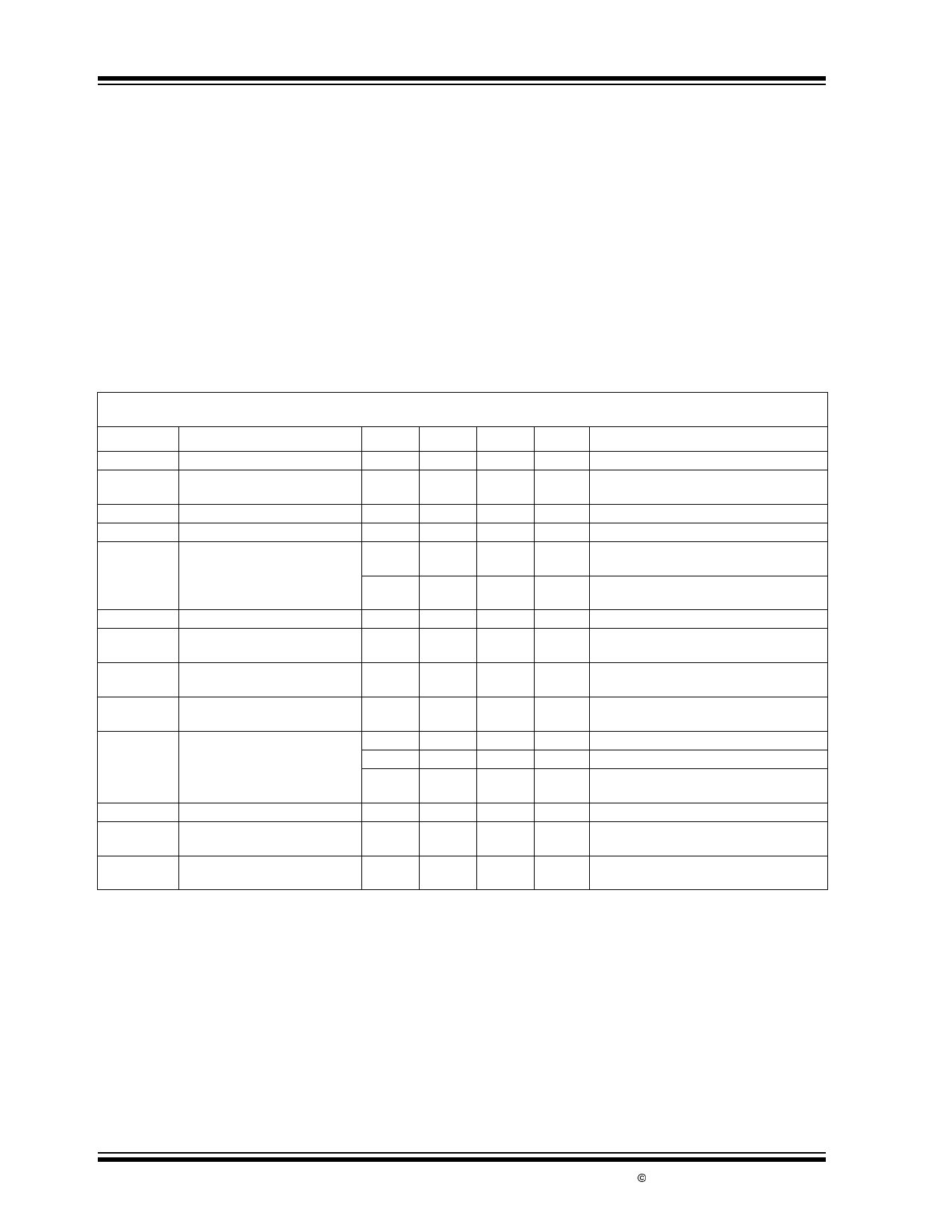
TC1266 ELECTRICAL SPECIFICATIONS
Electrical Characteristics: TA = +25°C, VIN = 5V, VAUX = 3.3V, IOUT = 0.1mA, COUT = 4.7µF, unless otherwise noted. Boldface
type specifications apply over full operating temperature range.
Symbol
Parameter
Min
Typ
Max Units
Test Conditions
VIN
IGND
IVIN
VAUX
IQ(AUX)
Supply Voltage
Ground Current
Reverse Leakage from VAUX
Supply Voltage
Quiescent Current
4.3
5.0
5.5
V
VAUX = 0V
—
230
450
µA VAUX = 0V (Note 6)
—
260
500
VAUX = 3.3V (Note 6)
—
-0.1
-1.0
µA VAUX = 3.6V, VIN = 0V, IOUT = 0mA
3.0
3.3
3.6
V
—
50
70
µA VIN = 0V, IOUT = 0mA
—
—
100
—
60
80
µA VIN = 5V, IOUT= 0mA
—
—
120
IVAUX
VTH(LO)
Reverse Leakage from VIN
5V Detector
Low Threshold Voltage
—
-0.1
-1.0
—
3.90
—
3.75
—
4.05
µA VIN = 5,5V, VAUX = 0V, IOUT = 0mA
V VIN Falling (Notes 2, 3)
VHYST
5V Detector
Hysteresis Voltage
—
260
—
mV (Notes 2, 3)
200
—
300
VTH(HI)
5V Detector
High Threshold Voltage
—
4.15
—
4.0
—
4.30
V VIN Rising (Notes 2, 3)
VOUT
LDO Output Voltage
IOUT
REG(LINE)
Output Current
Line Regulation
—
3.234
3.000
3.300
—
—
—
3.366
—
200
—
—
—
0.05
—
-0.5
—
0.5
V IOUT = 20mA
4.3V ≤ VIN ≤ 5.5V, 0mA ≤ IOUT ≤ 200mA
3.75V ≤ VIN ≤ 4.3V,
0mA ≤ IOUT ≤ 200mA (Note 4)
mA
% VIN = 4.3V to 5.5V
REG(LOAD) Load Regulation
—
0.05
—
-0.5
—
0.5
% IOUT= 0.1mA to 200mA
Note
1: Ensured by design.
2: See 5V Detect Thresholds, Figure 4-1.
3: Recommended source impedance for 5V supply: ≤ 0.25Ω. This will ensure that IOUT x RSOURCE < VHYST, thus avoiding DR toggling during
5V detect threshold transitions.
4: In Application Circuit, Figure 3-1.
5: See Timing Diagram, Figure 4-2.
6: Ground Current is independent of ILOAD.
DS21377B-page 2
© 2002 Microchip Technology Inc.
Share Link: 