TC1072 Просмотр технического описания (PDF) - TelCom Semiconductor Inc => Microchip
Номер в каталоге
Компоненты Описание
производитель
TC1072
TelCom Semiconductor Inc => Microchip

TC1072 Datasheet PDF : 12 Pages
| |||
PRELIMINARY INFORMATION
100mA CMOS LDO WITH SHUTDOWN,
ERROR OUTPUT AND VREF BYPASS
TC1073
ABSOLUTE MAXIMUM RATINGS*
Input Voltage .................................................................7V
Output Voltage .................................. (– 0.3) to (VIN + 0.3)
Power Dissipation .................... Internally Limited (Note 7)
Operating Temperature .................... – 40°C < TJ < 125°C
Storage Temperature ............................ – 65°C to +150°C
Maximum Voltage On Any Pin .......... VIN + 0.3V to – 0.3V
*Stresses beyond those listed under "Absolute Maximum Ratings" may
cause permanent damage to the device. These are stress ratings only, and
functional operation of the device at these or any other conditions beyond
those indicated in the operational sections of the specifications is not
implied. Exposure to absolute maximum rating conditions for extended
periods may affect device reliability.
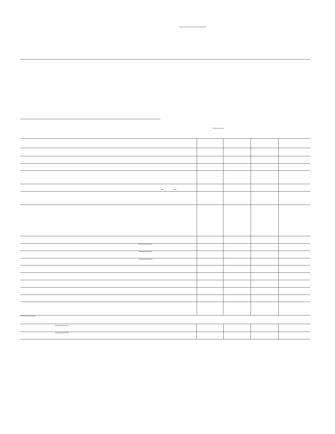
ELECTRICAL CHARACTERISTICS: VIN = VOUT + 1V, IL = 0.1mA, CL = 3.3µF, SHDN > VIH, TA = 25°C, unless otherwise noted.
Symbol
VIN
IOUTMAX
VOUT
TC VOUT
Parameter
Input Operating Voltage
Maximum Output Current
Output Voltage
VOUT Temperature Coefficient
∆VOUT/∆VIN
∆VOUT/VOUT
Line Regulation
Load Regulation
VIN – VOUT Dropout Voltage (Note 4)
IGND
IIN
IINSD
ROUT
PSRR
IOUTSC
∆VOUT/∆PD
TSD
∆TSD
eN
Ground Pin Current
Supply Current
Shutdown Supply Current
Output Resistance during Shutdown
Power Supply Rejection Ratio
Output Short Circuit Current
Thermal Regulation
Thermal Shutdown Die Temperature
Thermal Shutdown Hysteresis
Output Noise
SHDN Input
VIH
SHDN Input High Threshold
VIL
SHDN Input Low Threshold
Test Conditions
Min
Typ
Max
Note 9
Note 9
Notes 1, 9
Note 2, 9
—
100
VR – 2.5%
(VR + 1V) < VIN < 6V
IL = 0.1mA to IOUTMAX
(Note 3)
IL = 0.1mA
IL = 20mA
IL = 50mA
IL =100mA
(Note 4)
IL = IOUTMAX, (Note 5, 9)
SHDN = VIH, IL = 0
SHDN = 0V
SHDN < VIL
FRE ≤ 1kHz
VOUT = 0V
Note 6
IL = IOUTMAX
470pF from Bypass to GND
—
—
—
—
—
—
100 x VR
—
—
—
—
—
—
—
—
VR ±0.5%
20
40
0.05
0.5
20
70
100
200
0
50
—
160 x VR
64
300
0.04
160
10
260
6.5
—
VR + 2.5%
—
—
—
—
—
80
0.05
—
—
500
—
—
—
—
VIN = 2.5V to 6.5V
VIN = 2.5V to 6.5V
45
—
—
—
—
15
Units
V
mA
V
ppm/°C
%
%
mV
µA
µA
µA
kΩ
dB
mA
%/W
°C
°C
nV/√Hz
%VIN
%VIN
TC1073-01 6/5/97
2
Share Link: