TC1041 Просмотр технического описания (PDF) - Microchip Technology
Номер в каталоге
Компоненты Описание
производитель
TC1041
Linear Building Block – Dual Low Power Comparator and Voltage Reference with Programmable Hysteresis
Microchip Technology

TC1041 Datasheet PDF : 14 Pages
| |||
TC1041
1.0 ELECTRICAL
CHARACTERISTICS
ABSOLUTE MAXIMUM RATINGS*
Supply Voltage ......................................................6.0V
Voltage on Any Pin .......... (VSS – 0.3V) to (VDD + 0.3V)
Junction Temperature....................................... +150°C
Operating Temperature Range............. -40°C to +85°C
Storage Temperature Range .............. -55°C to +150°C
*Stresses above those listed under "Absolute Maximum
Ratings" may cause permanent damage to the device. These
are stress ratings only and functional operation of the device
at these or any other conditions above those indicated in the
operation sections of the specifications is not implied.
Exposure to Absolute Maximum Rating conditions for
extended periods may affect device reliability.
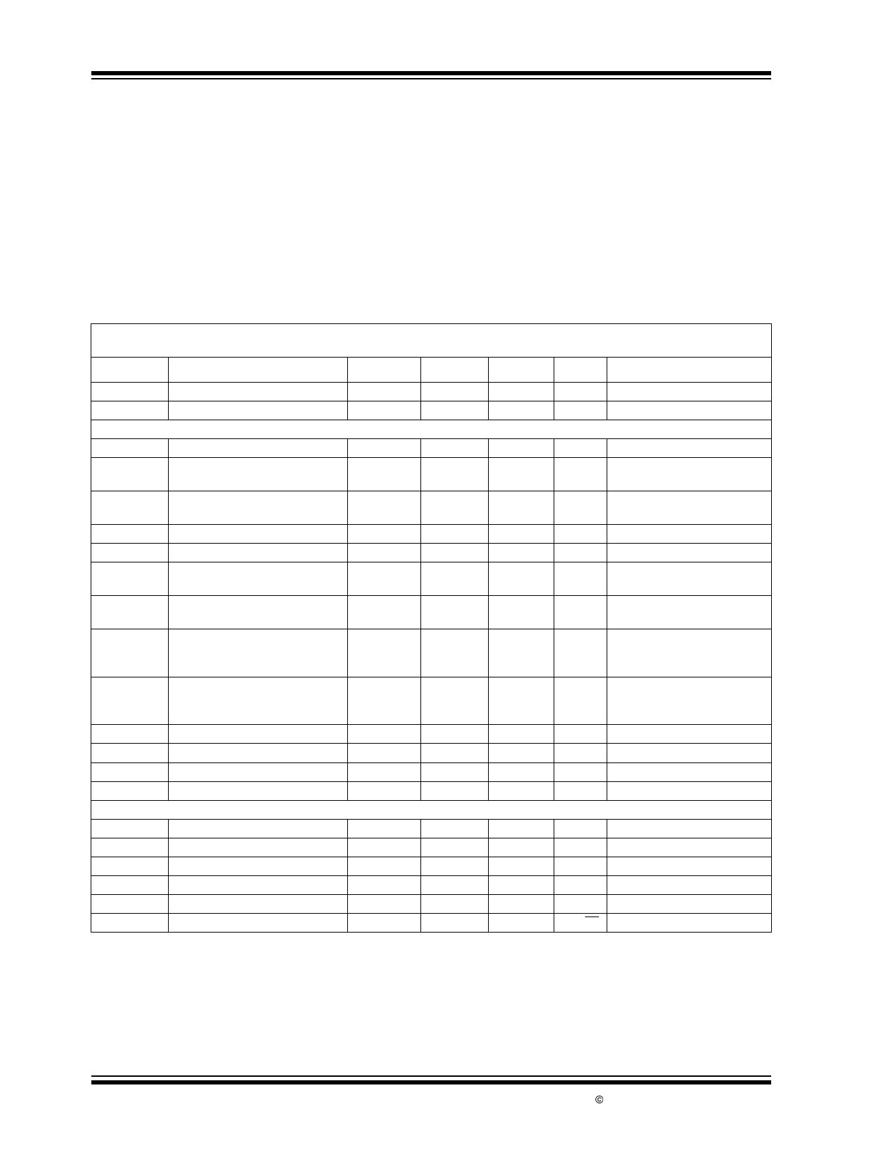
TC1041 ELECTRICAL SPECIFICATIONS
Electrical Characteristics: Typical values apply at 25°C and VDD = 3.0V. Minimum and maximum values apply for TA = -40° to
+85°C and VDD = 1.8V to 5.5V, unless otherwise specified.
Symbol
Parameter
Min
Typ
Max
Units
Test Conditions
VDD
Supply Voltage
IQ
Supply Current Operating
Comparators
1.8
—
5.5
V
—
10
15
µA All Outputs Open
VIR
IN+ Voltage Range
VSS – 0.2
—
VDD + 0.2
V
VOS
Input Offset Voltage
-5
—
+5
mV VDD = 3V, TA = 25°C
-5
+5
mV TA = -40°C to 85°C (Note 1)
IB
Input Bias Current
—
—
±100
pA TA = 25°C,
IN+ = VDD to VSS
VOH
Output High Voltage
VDD – 0.3
—
—
V
RL = 10kΩ to VSS
VOL
Output Low Voltage
—
—
0.3
V
RL = 10kΩ to VDD
CMRR
Common Mode Rejection Ratio
66
—
—
dB TA = 25°C, VDD = 5V
VCM = VDD to VSS
PSRR
Power Supply Rejection Ratio
60
—
—
dB TA = 25°C
VDD = 1.8V to 5V
ISRC
Output Source Current
1
—
—
mA IN+ = VDD,
Output Shorted to VSS
VDD = 1.8V
ISINK
Output Sink Current
2
—
—
mA IN+ = VSS,
Output Shorted to VDD
VDD = 1.8V
VHYST
Voltage Range at HYST Pin
VREF – 0.08
—
VREF
V
IHYST
Hysteresis Input Current
—
—
±100
nA
tPD1
Response Time
—
4
—
µsec 100mV Overdrive, CL = 100pF
tPD2
Response Time
—
6
—
µsec 10mV Overdrive, CL = 100pF
Voltage Reference
VREF
Reference Voltage
1.176
1.200
1.224
V
IREF(SOURCE) Source Current
50
—
—
µA
IREF(SINK)
Sink Current
50
—
—
µA
CL(REF)
Load Capacitance
—
—
100
pF
EVREF
Noise Voltage
—
20
—
µVRMS 100Hz to 100kHz
eVREF
Noise Voltage Density
—
1.0
—
µV/√Hz 1kHz
Note 1: VOS is measured as (VUT + VLT – 2VREF)/2 where VUT is the upper hysteresis threshold and VLT is the lower hysteresis threshold with
VREF – VHYST set to 10mV. This represents the assymetry of the hysteresis thresholds around VREF.
DS21346B-page 2
© 2002 Microchip Technology Inc.
Share Link: