TB2905HQ –ü—Ä–æ—Å–º–æ—Ç—Ä —Ç–µ—Ö–Ω–∏—á–µ—Å–∫–æ–≥–æ –æ–ø–∏—Å–∞–Ω–∏—è (PDF) - Toshiba
–ù–æ–º–µ—Ä –≤ –∫–∞—Ç–∞–ª–æ–≥–µ
–ö–æ–º–ø–æ–Ω–µ–Ω—Ç—ã –û–ø–∏—Å–∞–Ω–∏–µ
–ø—Ä–æ–∏–∑–≤–æ–¥–∏—Ç–µ–ª—å
TB2905HQ Datasheet PDF : 17 Pages
| |||
Operational Description (Each description applies to a single channel)
TB2905HQ
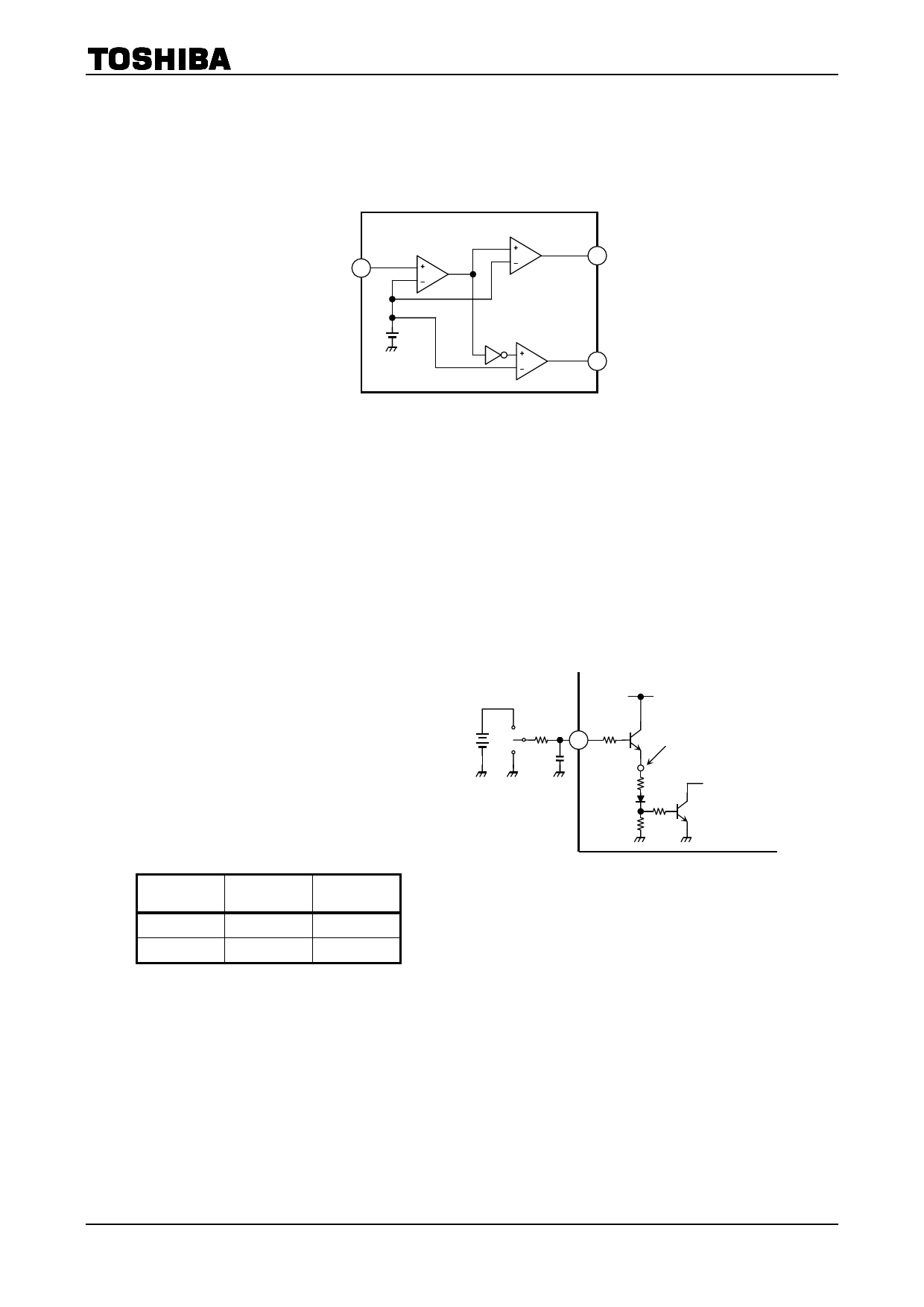
1. Voltage Gain
The TB2905HQ has no NF (negative feedback) pins. Therefore, the voltage gain (GV) is determined
within the IC.
Input
Amplifier 1
Amplifier 2A
Amplifier 2B
Figure 1 Amplifier Configuration
Voltage gain of amplifier 1: GV1 = 0 dB
Voltage gain of amplifiers 2A and 2B: GV2 = 20 dB
Voltage gain obtained by BTL connection: GV (BTL) = 6 dB
Therefore, the total voltage gain is determined by the following expression:
GV = GV1 + GV2 + GV (BTL) = 0 + 20 + 6 = 26dB
Although this configuration without an NF pin does not allow the user to adjust voltage gain, it
eliminates the need for an NF capacitor, resulting in lower total application cost and smaller mounting
space.
2. Standby Switching Function (Pin 4)
The TB2905HQ can be powered up or
down by controlling the state of pin 4
(standby pin).
The threshold voltage for pin 4 is
approximately 3 VBE (typ.). The supply
current in standby state is approximately 2
µA (typ.).
ON Power
OFF
10 kΩ
4
VCC
≈ 2 VBE
To bias
cutoff circuit
Pin 4 control voltage: VSB
Stand-by
ON
OFF
Power
OFF
ON
VSB (V)
0~0.5
2.5~6 V
Figure 2 Driving pin 4 high powers up
the TB2905HQ
When changing the time constant for pin 4, check the pop noise produced.
< Advantages of standby switching >
(1) The microcontroller can directly turn VCC on or off without using a switching relay.
(2) Since the control current is microscopic, a switching relay with small current capacity is satisfactory
for switching.
3
2005-08-17
Share Link: 