TA8492P(2001) Просмотр технического описания (PDF) - Toshiba
Номер в каталоге
Компоненты Описание
производитель
TA8492P Datasheet PDF : 11 Pages
| |||
Handling Precautions
TA8492P
(CW/CCW/Stop control circuit)
a) At 3ST input, because the input voltage ranges for VRV (Reverse mode) and VSTP (Stop mode) are narrow,
make sure no impedance is caused between the IC VCC and GND pins. Do not connect an input resistor to
the 3ST pin because it causes voltage offset.
b) When controlling the rotation direction using 3ST input, switch the direction from Reverse to Stop mode or
vice versa with VS = 0 V, because punch-through current may be generated at output.
(Hall amp. circuit)
A Hall IC input amplitude of over 400 mVp-p causes an output function error. Make sure the amplitude is
within the specified range.
(Output circuit)
Utmost care is necessary in the design of the output fine, VS, VCC and GND line since IC may be destroyed due
to short-circuit between output air contamination fault, or fault by improper grounding
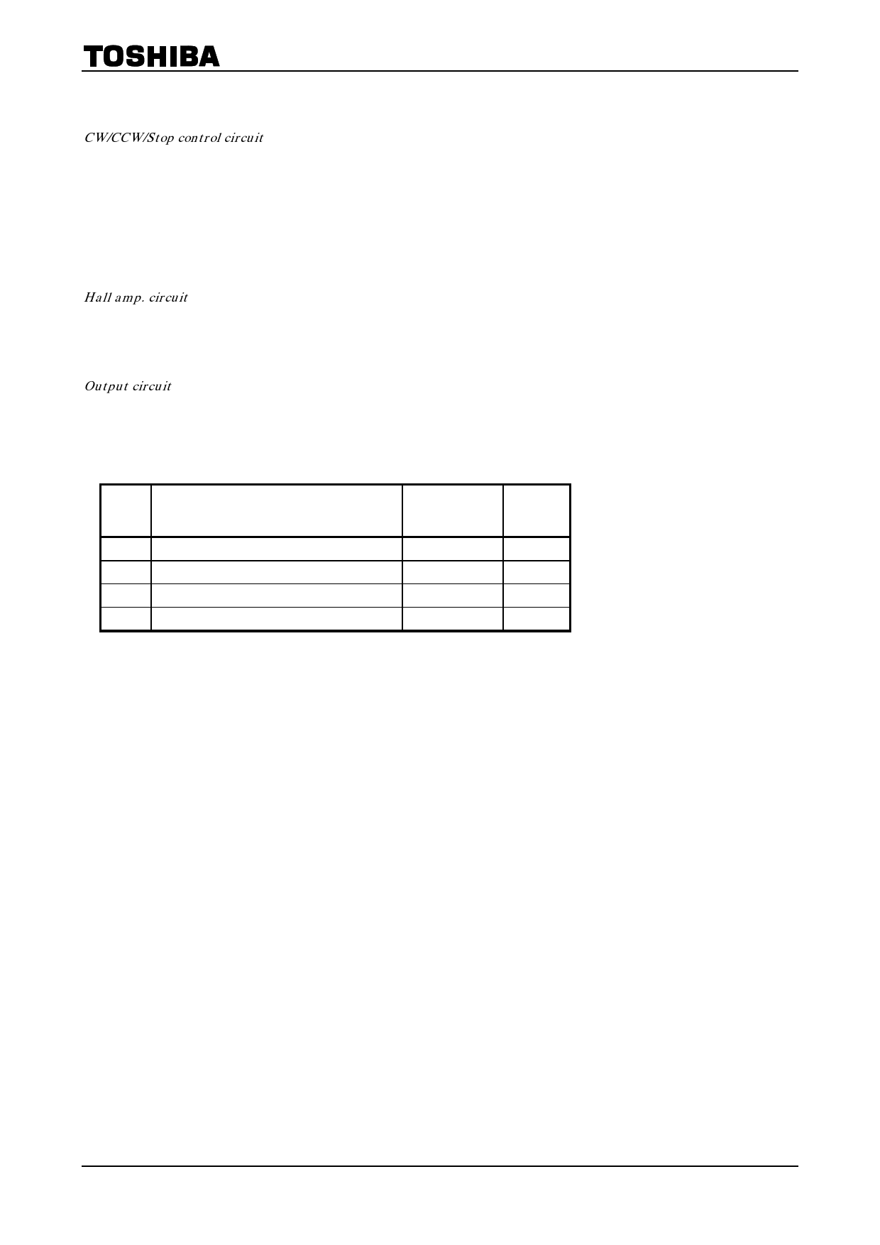
External parts
Symbol
Function
Recommended Remarks
Value
C1 Power supply line oscillation prevention
C2 Power supply line oscillation prevention
C3 Output noise reduction
R1 Hall bias
4.7 µF
4.7 µF
4.7 µF
(Note 3)
(Note 4)
Note 3: Set an appropriate value depending on the motor and use conditions.
Set an appropriate value so that the Hall IC output common mode input voltage and amplitude fall within the
specified ranges in the Electrical Characteristics table.
Note 4: Be sure to set this bias so that the Hall element output amplitude and common mode input voltage fall within
the ranges specified in the table of electrical characteristic.
2001-02-01 5/11
Share Link: 