SY88923V Просмотр технического описания (PDF) - Micrel
Номер в каталоге
Компоненты Описание
производитель
SY88923V Datasheet PDF : 6 Pages
| |||
Micrel, Inc.
SY88923V
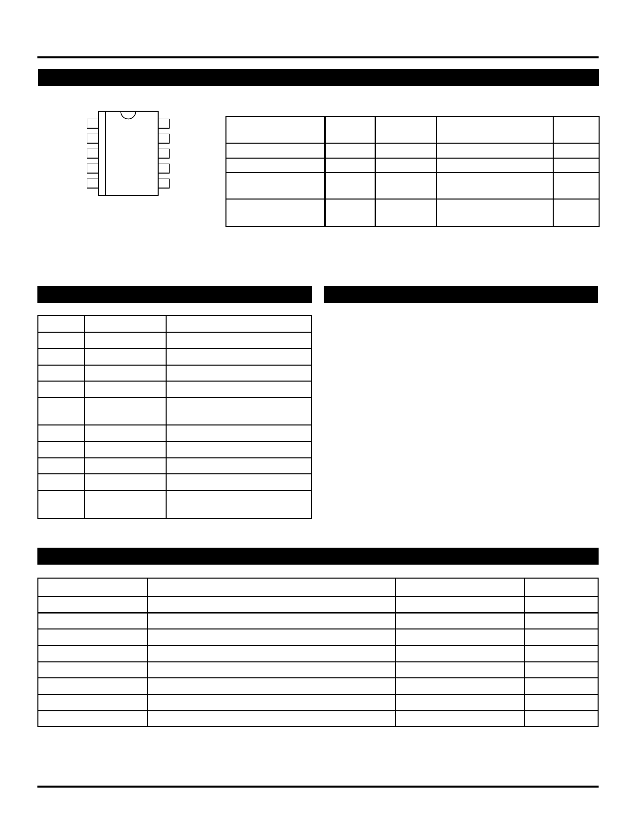
PACKAGE/ORDERING INFORMATION
/EN 1
DIN 2
/DIN 3
VREF 4
LOSLVL 5
MSOP
K10-1
10 VCC
9 DOUT
8 /DOUT
7 LOS
6 GND
10-Pin MSOP (K10-1)
Ordering Information(1)
Part Number
Package Operating
Type
Range
Package
Marking
Lead
Finish
SY88923VKC
SY88923VKCTR(2)
SY88923VKG(3)
SY88923VKGTR(2, 3)
K10-1
K10-1
K10-1
K10-1
Commercial
Commercial
Industrial
Industrial
923V
923V
923V with
Pb-Free bar-line indicator
923V with
Pb-Free bar-line indicator
Sn-Pb
Sn-Pb
Pb-Free
NiPdAu
Pb-Free
NiPdAu
Notes:
1. Contact factory for die availability. Dice are guaranteed at TA = 25°C, DC Electricals only.
2. Tape and Reel.
3. Pb-Free package is recommended for new designs.
PIN NAMES
GENERAL DESCRIPTION
Pin
DIN
/DIN
LOSLVL
/EN
LOS
GND
/DOUT
DOUT
VCC
VREF
Type
Data Input
Data Input
Input
TTL Input
TTL Output
(Open Collector)
Ground
PECL Output
PECL Output
Power Supply
Output
Function
Data Input
Inverting Data Input
LOS Limit Set
Output Enable (Active Low)
Loss of Signal Indicator
(Active High)
Ground
Inverting Data Output
Data Output
Positive Power Supply
Reference Voltage Output for
LOS Level Set (see Fig. 3)
General
The SY88923V is an integrated limiting amplifier intended
for high-frequency fiber-optic applications. The circuit
connects to typical trans-impedance amplifiers found within
a fiber-optics link. The linear signal output from a trans-
impedance amplifier can contain significant amounts of noise,
and may vary in amplitude over time. The SY88923V limiting
amplifier quantizes the signal and outputs a voltage-limited
waveform.
The /EN pin allows the user to disable the output signal
without removing the input signal.
ABSOLUTE MAXIMUM RATINGS(1)
Symbol
Rating
Value
Unit
VCC
Power Supply Voltage
0 to +7.0
V
DIN, /DIN
DOUT, /DOUT
Input Voltage
Output Voltage (with 50Ω load)
0 to VCC
V
VCC –2.5 to VCC +0.3
V
/EN
LOSLVL
Input Voltage
Input Voltage
0 to VCC
V
0 to VCC
V
VREF
TA
Tstore
Output Voltage
Operating Temperature Range
Storage Temperature Range
VCC –2.0 to VCC
V
–40 to +85
°C
–55 to +125
°C
Note:
1. Permanent device damage may occur if absolute maximum ratings are exceeded. This is a stress rating only and functional operation is not implied at
conditions other than those detailed in the operational sections of this data sheet. Exposure to absolute maximum ratlng conditions for extended periods
may affect device reliability.
M9999-051706
hbwhelp@micrel.com or (408) 955-1690
2
Share Link: 