SX1240 Просмотр технического описания (PDF) - Semtech Corporation
Номер в каталоге
Компоненты Описание
производитель
SX1240 Datasheet PDF : 20 Pages
| |||
ADVANCED COMMUNICATIONS & SENSING
SX1240
Integrated Transmitter IC
DATASHEET
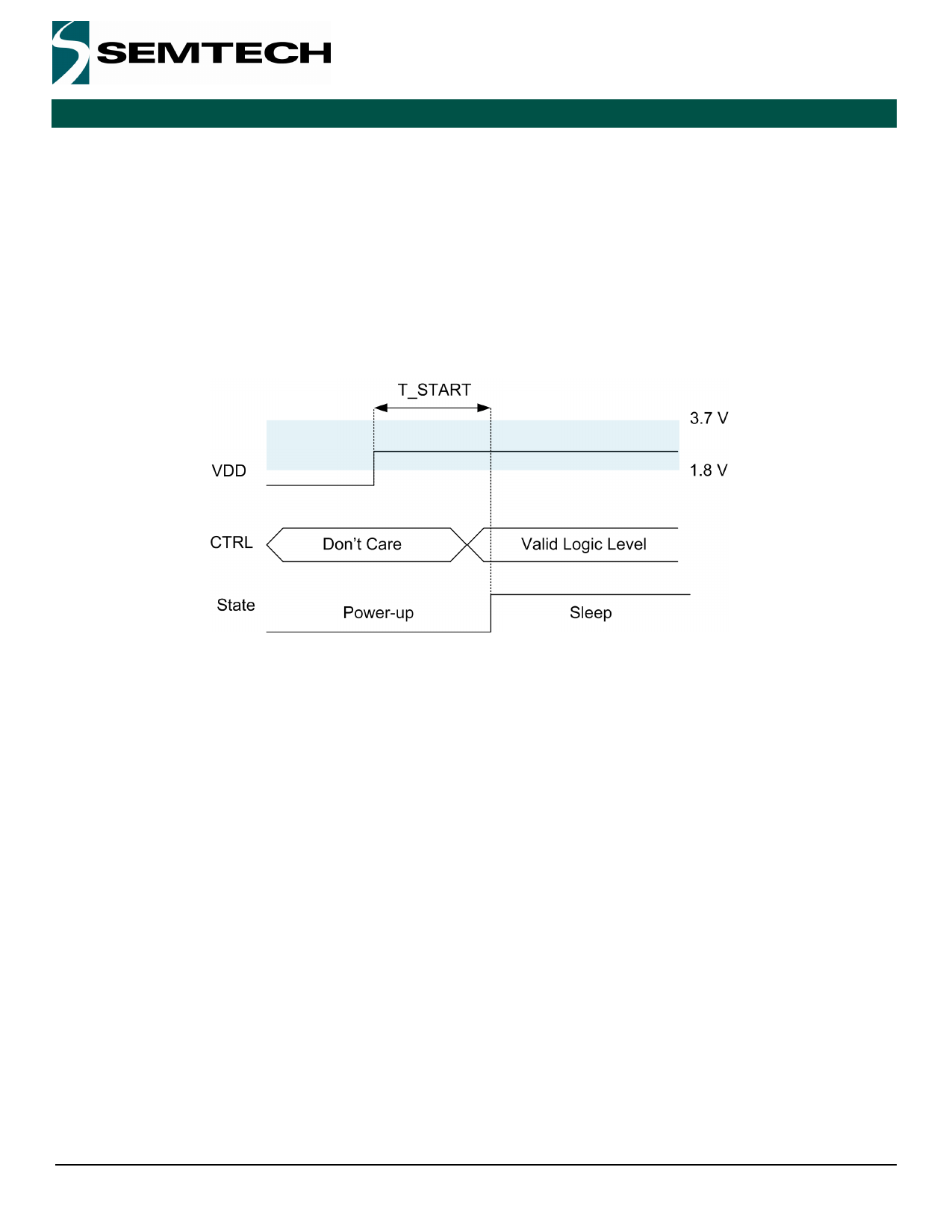
When powering up the circuit (microcontroller and SX1240), the logic level of the CTRL pin is sampled after T_START, as
described on Figure 3. During T_START, the microcontroller IO driving the CTRL pin must be configured as an output,
driving the CTRL pin to the desired state.
Note
whilst the logic level of CTRL pin during T_START (initialization phase of the microcontroller) does not have any
effect on the device operation, the pin should not be connected to VDD through an impedance lower than 20 k
ohms or higher than 1 M ohms.
Figure 7. Power-up Timing
3.2.2. Transmitter Operation in Advanced Mode
When operating in advanced mode two possibilities exist for operation of the transmitter, these are dependent upon the
state of the Tx Mode bit (D12 of the register description in Table 8).
Tx Mode = ‘0’
When set to logical ‘0’ operation is identical to that of the Power & Go mode, following completion of the programming
phase, the SX1240 will be placed in transmit mode upon the next rising edge detected on the DATA pin. Transmit operation
will then be in accordance with that of Figure 4 with the time TOFFT corresponding to that programmed.
Note that prior to programming the default, logical ‘0’, configuration is loaded. Note also that subsequent programming
iterations can only be performed once the transmit cycle is finished - including the time required for switching off the PA
(TOFFT).
Tx Mode = ‘1’
With Tx Mode (D12) set to ‘1’ during the register programming cycle detailed in Figure 5, the SX1240 is placed directly in
transmit mode. It will then remain in transmit mode until a second TWI register write operation where, if reset to logical ‘0’,
the SX1240 returns to sleep mode. An illustration of this operation is shown in the following timing diagram.
Please also note that once in sleep mode, subsequent activity on the DATA pin (without clocking of the CTRL line) will
trigger transmission in accordance with Figure 4. Care must hence be taken to avoid inadvertent transmission due to such
activity.
SX1240, Rev 1, Oct 2010
©2010 Semtech Corp.
Page 11
www.semtech.com
Share Link: 