SW65-0440 Просмотр технического описания (PDF) - M/A-COM Technology Solutions, Inc.
Номер в каталоге
Компоненты Описание
производитель
SW65-0440 Datasheet PDF : 6 Pages
| |||
SW65-0440
GaAs SP4T Switch, Absorptive, Single Supply
DC - 3.0 GHz
Rev. V7
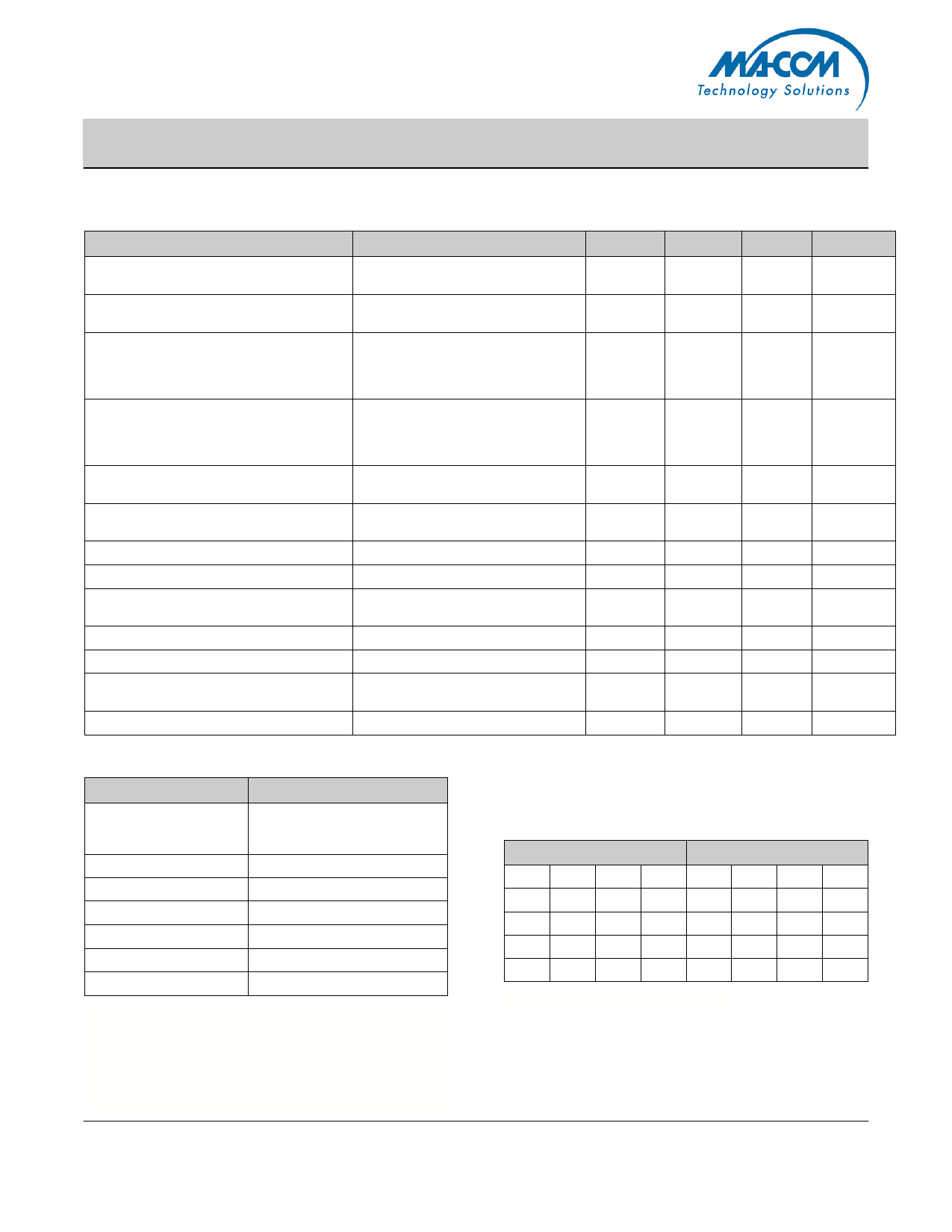
Electrical Specifications: TA = 25°C
Parameter
Insertion Loss
Isolation
VSWR
RF1-RF4 On
RF1- RF4 Off
RFC
RFC
Switching Speed1
Trise Tfall
Ton
Toff
Transients
1 dB Compression
Input IP3
VCC
VEE
VIL
VIH
lin (Input Leakage Current)
Icc (Quiescent Supply Current)
ΔIcc
(Additional Supply Current Per TTL Input Pin)
IEE
Test Conditions
DC - 2.0 GHz
DC - 3.0 GHz
DC - 2.0 GHz
DC - 3.0 GHz
DC - 3.0 GHz
DC - 3.0 GHz
DC - 2.0 GHz
DC - 3.0 GHz
10%/90%, 90%/10%
50% TTL to 90%/10% RF
In-band (peak to peak)
.05 GHz
.5 - 3.0 GHz
Two tone inputs 0.05 GHz
up to +5 dBm 0.5 - 3.0 GHz
—
—
LOW-level input voltage
HIGH-level input voltage
Vin = VCC or GND
Vcntrl = VCC or GND
VCC = Max, Vcntrl = VCC - 2.1 V
VEE min to max, Vin = VIL or VIH
Units
dB
dB
dB
dB
Ratio
Ratio
Ratio
Ratio
ns
ns
mV
dBm
dBm
dBm
dBm
V
V
V
V
uA
uA
mA
mA
Min
—
—
32
25
—
—
—
—
—
—
—
—
—
—
—
+4.5
-8.0
0.0
2.0
-1.0
—
—
-1.0
Typ
1.2
1.3
35
29
1.2:1
1.4:1
1.2:1
1.6:1
15
50
50
+20
+27
+35
+46
+5.0
-5.0
—
—
—
250
—
-0.2
Max
1.8
2.5
—
—
1.6:1
1.8:1
1.5:1
2.2:1
50
150
150
—
—
—
—
+5.5
-4.75
0.8
5.0
1.0
400
1.0
—
Absolute Maximum Ratings 2,3,4
1. Decoupling capacitors (.1 µF) are required on the power supply lines.
Parameter
Absolute Maximum
Max. Input Power
0.05 GHz
+27 dBm
Truth Table (Switch)
0.5 - 3.0 GHz
VCC
VEE
VCC - VEE
Vin5
Operating Temperature
+34 dBm
-0.5V ≤ VCC ≤ +7.0V
-8.5V ≤ VEE ≤ +0.5V
-0.5V ≤ VCC - VEE ≤ 14.5V
-0.5V ≤ Vin ≤ VCC + 0.5V
-40ºC to +85ºC
TTL
RF Common To:
C1 C2 C3 C4 RF1 RF2 RF3 RF4
1
0
0
0
On Off Off Off
0
1
0
0
Off On Off Off
0
0
1
0
Off Off On Off
0
0
0
1
Off Off Off On
Storage Temperature
-65ºC to +125ºC
2. Exceeding any one or combination of these limits may cause
0 = TTL Low; 1 = TTL High
permanent damage to this device.
3. M/A-COM does not recommend sustained operation near
these survivability limits.
4. When the RF input is applied to the terminated port, the
absolute maximum power is +30 dBm.
5. Standard CMOS TTL interface, latch-up will occur if logic
signal is applied prior to power supply.
2
ADVANCED: Data Sheets contain information regarding a product M/A-COM Technology Solutions • North America Tel: 800.366.2266 • Europe Tel: +353.21.244.6400
is considering for development. Performance is based on target specifications, simulated results,
and/or prototype measurements. Commitment to develop is not guaranteed.
PRELIMINARY: Data Sheets contain information regarding a product M/A-COM Technology
• India Tel: +91.80.4155721
• China Tel: +86.21.2407.1588
Visit www.macomtech.com for additional data sheets and product information.
Solutions has under development. Performance is based on engineering tests. Specifications are
typical. Mechanical outline has been fixed. Engineering samples and/or test data may be available. M/A-COM Technology Solutions Inc. and its affiliates reserve the right to make
Commitment to produce in volume is not guaranteed.
changes to the product(s) or information contained herein without notice.
Share Link: 