STLVDS051 Просмотр технического описания (PDF) - STMicroelectronics
Номер в каталоге
Компоненты Описание
производитель
STLVDS051 Datasheet PDF : 11 Pages
| |||
STLVDS051
RECEIVER SWITCHING CHARACTERISTICS (Typical values are at TA = 25°C, VCC = 3.3V ±10%,
TA = -40 to 85°C unless otherwise specified)
Symbol
Parameter
Test Conditions
Min. Typ. Max. Unit
tPLH
tPHL
tr
tf
tsk(P)
tPZH
tPZL
tPHZ
tPLZ
Propagation Delay Time,
Low to High Output
Propagation Delay Time,
High to Low Output
Differential Output Signal
Rise Time
Differential Output Signal
Fall Time
Pulse Skew (|tTHL - tTLH|)
(Note 1)
Propagation Delay Time,
High Impedance to High
Level Output
Propagation Delay Time,
High Impedance to Low
Level Output
Propagation Delay Time,
High Level to High
Impedance Output
Propagation Delay Time,
Low Level to High
Impedance Output
CL = 10pF
3.0
4.0
ns
3.0
4.0
ns
0.6
1
ns
0.6
1
ns
0.25
ns
2.5
ns
2.5
ns
7
ns
4
ns
Note 1: tsk(P) is the magnitude of the time difference between the high to low and low to high propagation delay times at an output
Note 2: tsk(O) is the magnitude of the time difference between the output of a single device with all their inputs connected together.
Note 3: tsk(PP) is the magnitude of the difference between any specified terminals of two devices when both devices operate with the same
supply voltages, same temperature, and have identical packages and test circuit.
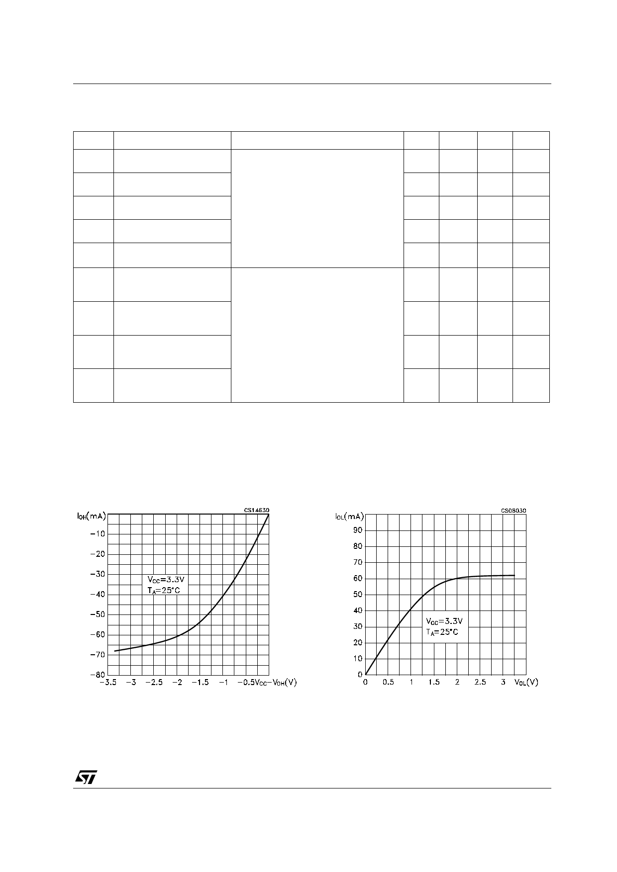
TYPICAL PERFORMANCE CHARACTERISTICS (unless otherwise specified TJ = 25°C)
Figure 1 : Output Current vs Output High Voltage
for Receiver
Figure 2 : Output Current vs Output Low Voltage
for Receiver
5/11
Share Link: 