STK6005 Просмотр технического описания (PDF) - Unspecified
Номер в каталоге
Компоненты Описание
производитель
STK6005 Datasheet PDF : 36 Pages
| |||
STK6005
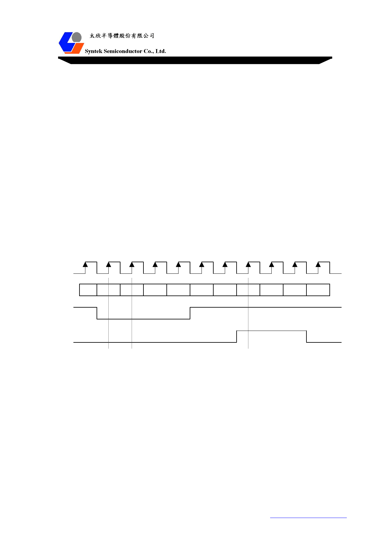
5. FUNCTION
5.1 Input Timing and Format
This chip supports a 24-bit RGB input (up to SXGA 75Hz) of a single port, a 16-bit YUV 4:2:2 input,
and an 8-bit YUV 4:2:2 (CCIR-656) video input. The timing diagrams are provided below.
For RGB input format, the RGB data (RIN/GIN/BIN ports) and H-Sync (HSI), V-Sync (VSI) are
sampled at the rising or falling edge of VCLK.
For TMDS input format, a control signal ExtDE can be provided to define the valid data.
For video input format, the input YUV ports are shared with RIN/GIN/BIN ports. The 16-bit YUV 4:2:2
format uses RIN[7:0] for Y[7:0], GIN[7:0] for UV[7:0], and BIN[7:1] for YUV control bus. Hsync / Vsync
are used as H-Sync and V-Sync input signals. Cref is used as a clock edge qualifier. Href and Vref are
used to define the valid data. Field input is used as the odd / even fields indicator.
The 8-bit YUV 4:2:2 (CCIR-656) format uses RIN[7:0] for data input YUV[7:0], and the timing control is
also embedded in the data stream. Therefore, there are no control signal connections needed for this
format.
VCLK
R/G/BIN
HSI/VSI
ExtDE
RGB0 RGB1 RGB2
RGB input format timing diagram
10
Back to Contents Table
Share Link: 