STA506 Просмотр технического описания (PDF) - STMicroelectronics
Номер в каталоге
Компоненты Описание
производитель
STA506 Datasheet PDF : 14 Pages
| |||
STA506
3 TECHNICAL INFO:
The STA506 is a dual channel H-Bridge that is able to deliver more than 60W per channel (@ THD=10%) of
audio output power in high efficiency.
The STA506 converts both DDX and binary-controlled PWM signals into audio power at the load. It includes a
logic interface , integrated bridge drivers, high efficiency MOSFET outputs and thermal and short circuit protec-
tion circuitry.
In DDX mode, two logic level signals per channel are used to control high-speed MOSFET switches to connect
the speaker load to the input supply or to ground in a Bridge configuration, according to the damped ternary
Modulation operation.
In Binary Mode operation , both Full Bridge and Half Bridge Modes are supported. The STA506 includes over-
current and thermal protection as well as an under-voltage
Lockout with automatic recovery. A thermal warning status is also provided.
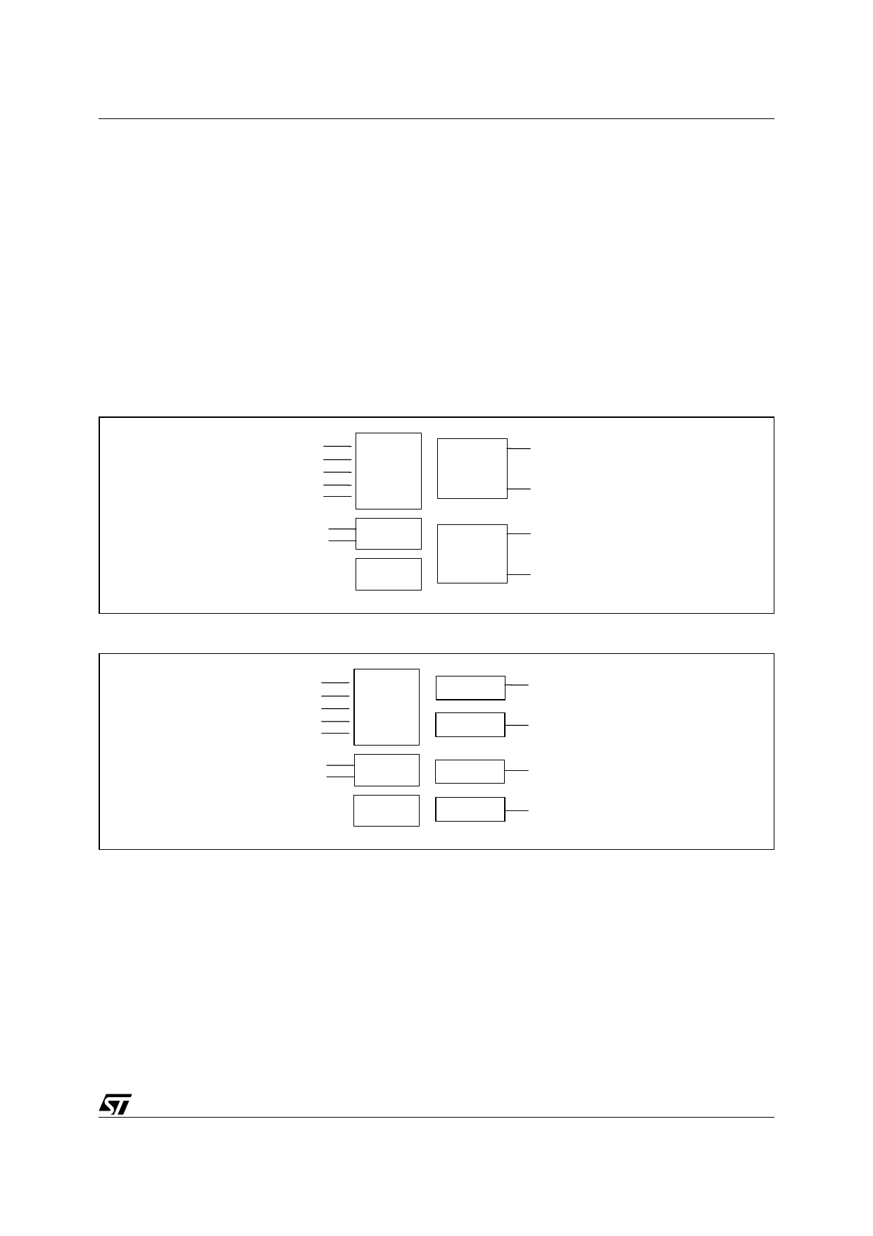
Figure 6. STA506 Block Diagram Full-Bridge DDX® or Binary Modes
INL[1:2]
INR[1:2]
VL
PWRDN
TRI-STATE
FAULT
TWARN
Logic I/F
and Decode
Left
H-Bridge
Protection
Circuitry
Regulators
Right
H-Bridge
OUTPL
OUTNL
OUTPR
OUTNR
Figure 7. STA506 Block Diagram Binary Half-Bridge Mode
INL[1:2]
INR[1:2]
VL
PWRDN
TRI-STATE
FAULT
TWARN
Logic I/F
and Decode
Protection
Circuitry
Regulators
LeftA
‰-Bridge
LeftB
‰-Bridge
RightA
‰-Bridge
RightB
‰-Bridge
OUTPL
OUTNL
OUTPR
OUTNR
3.1 Logic Interface and Decode:
The STA506 power outputs are controlled using one or two logic level timing signals. In order to provide a proper
logic interface, the Vbias input must operate at the dame voltage as the DDX control logic supply.
3.2 Protection Circuitry:
The STA506 includes protection circuitry for over-current and thermal overload conditions. A thermal warning
pin (pin.28) is activated low (open drain MOSFET) when the IC temperature exceeds 130C, in advance of the
thermal shutdown protection. When a fault condition is detected , an internal fault signal acts to immediately
disable the output power MOSFETs, placing both H-Bridges in high impedance state. At the same time an open-
drain MOSFET connected to the fault pin (pin.27) is switched on.
7/14
Share Link: 