ST2329 Просмотр технического описания (PDF) - STMicroelectronics
Номер в каталоге
Компоненты Описание
производитель
ST2329 Datasheet PDF : 21 Pages
| |||
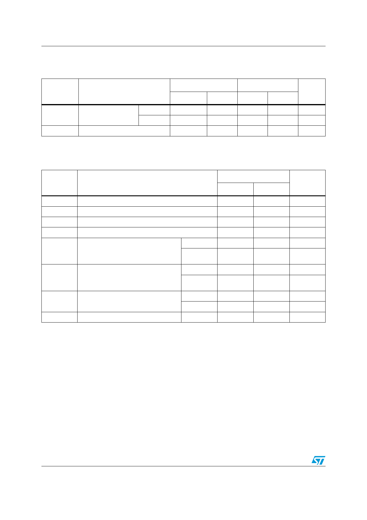
Electrical characteristics
ST2329
Table 8.
Symbol
AC characteristics - test conditions: VL = 2.5 −2.7 V (load CL = 15 pF; Rup = 4.7 kΩ; driver
tr = tf ≤ 2 ns) over temperature range -40 °C to 85 °C
Parameter
VCC = 2.7 −3.6 V
Min
Max
VCC = 4.3 − 5.5 V
Unit
Min
Max
tPZL tPZH Output enable and
En
tPLZ tPHZ disable time
Dis
6
6
ns
40
40
ns
DR
Data rate(1)
2.5
3.2
MHz
1. The data rate is guaranteed based on the condition that the output I/O signal rise/fall time is less than 15% of the input I/O
signal period; the input I/O signal is at 50% duty cycle and the output I/O signal duty cycle deviation not less than 30%.
Table 9.
Symbol
AC characteristics - test conditions: VL = 2.7 −3.6 V (load CL = 15 pF; Rup = 4.7 kΩ; driver
tr = tf ≤ 2 ns) over temperature range -40 °C to 85 °C
Parameter
VCC = 4.3 − 5.5 V
Unit
Min
Max
tRVCC Rise time I/OVCC
55
ns
tFVCC Fall time I/OVCC
3
ns
tRVL
Rise time I/OVL
4
ns
tFVL
Fall time I/OVL
3
ns
tI/OVL-VCC
Propagation delay time
I/OVL-LH to I/OVCC-LH
I/OVL-HL to I/OVCC-HL
tPLH
tPHL
2
ns
4
ns
tI/OVCC-VL
Propagation delay time
I/OVCC-LH to I/OVL-LH
I/OVCC-HL to I/OVL-HL
tPLH
tPHL
4
ns
4
ns
tPZL tPZH Output enable and disable time
En
tPLZ tPHZ
Dis
6
ns
40
ns
DR
Data rate(1)
2.8
MHz
1. The data rate is guaranteed based on the condition that the output I/O signal rise/fall time is less than 15% of the input I/O
signal period; the input I/O signal is at 50% duty cycle and the output I/O signal duty cycle deviation not less than 30%.
10/21
Share Link: 