CXA2039M Просмотр технического описания (PDF) - Sony Semiconductor
Номер в каталоге
Компоненты Описание
производитель
CXA2039M Datasheet PDF : 11 Pages
| |||
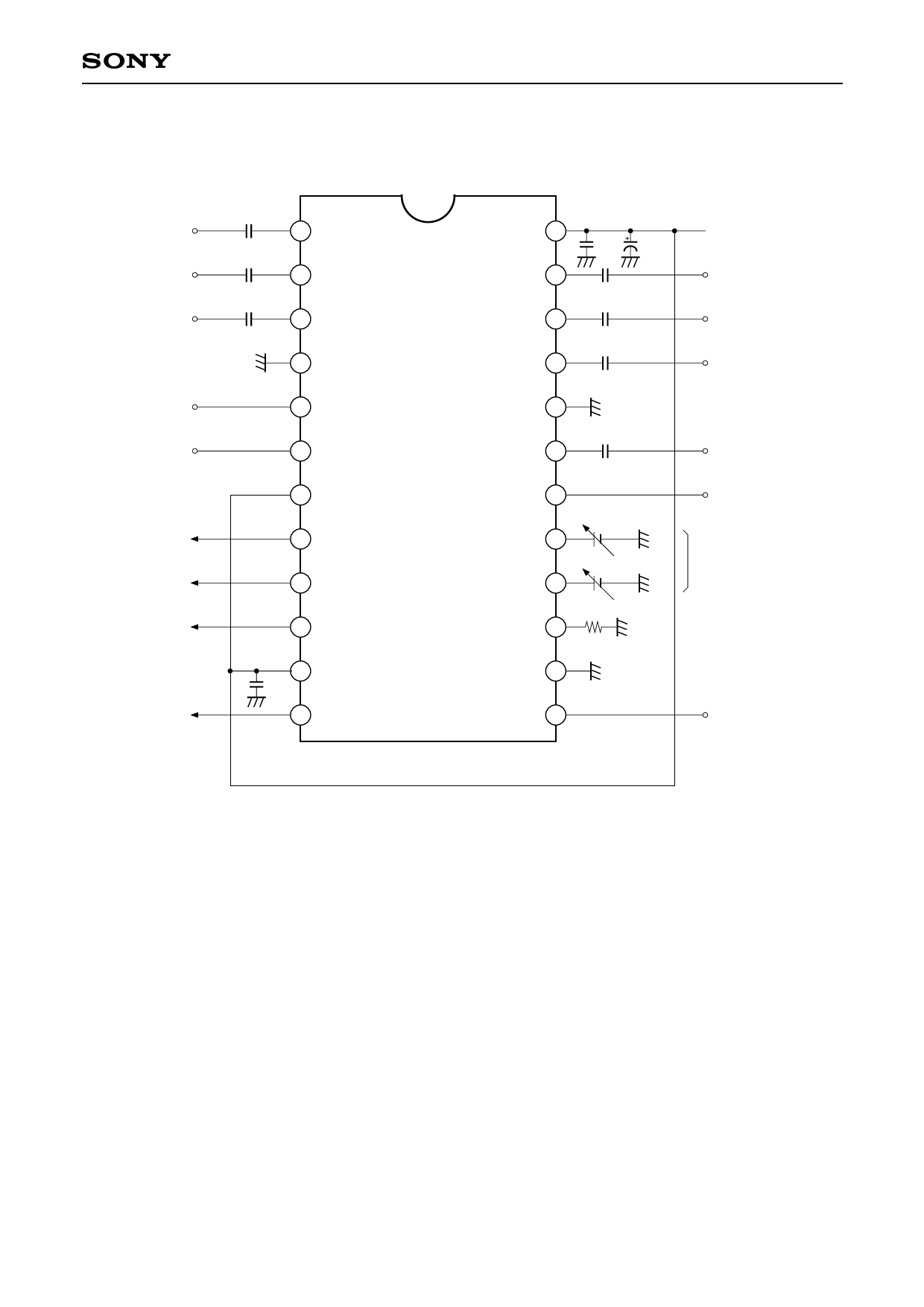
Application Circuit
Y1 input 0.1µ
R-Y1 input 0.1µ
B-Y1 input 0.1µ
1 Y1 IN
2 RY1 IN
3 BY1 IN
4 GND
Clamp Pulse input
Y/B-Y/R-Y
switching signal input
5 CLAMP
6 YUV SW
7 LEVEL
Y output
8 Y OUT
R-Y output
9 RY OUT
B-Y output
10 BY OUT
0.01µ
11 VCC
Main Y output
12 TV OUT
CXA2039M
0.01µ 47µ
VCC 24
Y2 IN 23
0.1µ
RY2 IN 22
0.1µ
BY2 IN 21
0.1µ
GND 20
TV IN 19
0.1µ
Y SW 18
HUE 17
COLOR 16
10k
DLY 15
Delay = 600ns
GND 14
DLY SW 13
9V
Y2 input
R-Y2 input
B-Y2 input
Main Y input
Y switching signal input
(TV IN and Y1 IN/Y2 IN
switching)
Control DC (0 to 9V)
Delay increases as
resistance increases
Delay on/off
signal input
Pin 7 (Pins 9, 10 and 12 output level switching)
9V = Output High MODE [RYOUT: –2.3dB (Typ.)/BYOUT: –4.7dB (Typ.)]
0V = Output Low MODE [RYOUT: –3.1dB (Typ.)/BYOUT: –5.3dB (Typ.)]
Application circuits shown are typical examples illustrating the operation of the devices. Sony cannot assume responsibility for
any problems arising out of the use of these circuits or for any infringement of third party patent and other right due to same.
–9–
Share Link: 