SPX1129M3-2.5 Просмотр технического описания (PDF) - Signal Processing Technologies
Номер в каталоге
Компоненты Описание
производитель
SPX1129M3-2.5 Datasheet PDF : 5 Pages
| |||
Also, it may be programmed for any output voltage between its
1.235V reference and its 30V maximum rating. As seen in
Figure 2, an external pair of resistors is required.
Refer to the below equation for the programming of the output
voltage:
VOUT = VREF × (1 + R1/ R2)+ IFBR1
The VREF is 1.235 and IFB is the feedback bias current, nominally
-20nA. The minimum recommended load current of 1 µA forces
an upper limit of 1.2 MΩ on value of R2. If no load is presented
the IFB produces an error of typically 2% in VOUT, which may be
eliminated at room temperature by trimming R1. To improve the
accuracy choose the value of R2 = 100k this reduces the error by
0.17% and increases the resistor program current by 12µA. Since
the SPX1129 typically draws 60 µA at no load with Pin 2 open-
circuited this is a small price to pay
SPX1129
REDUCING OUTPUT NOISE
It may be an advantage to reduce the AC noise present at the output.
One way is to reduce the regulator bandwidth by increasing the size of
the output capacitor. This is the only way that noise can be reduced
on the 3 lead SPX1129 but is relatively inefficient, as increasing the
capacitor from 1µF to 220µF only decreases the noise from 430µV to
160µV Vrms for a 100kHz bandwidth at 5V output.
Noise could also be reduced fourfold by a bypass capacitor across R1,
since it reduces the high frequency gain from 4 to unity. Pick
CBYPASS ≅ 1 / 2πR1 × 200 Hz
or choose 0.01µF. When doing this, the output capacitor must be
increased to 3.3µF to maintain stability. These changes reduce the
output noise from 430µV to 100µV Vrms for a 100kHz bandwidth at
5V output. With the bypass capacitor added, noise no longer scales
with output voltage so that improvements are more dramatic at higher
output voltages.
HEAT SINK REQUIREMENTS
Depending on the maximum ambient temperature and maximum
power dissipation a heat sink may be required with the SPX1129.
The junction temperature range has to be within the range
specified under Absolute Maximum Ratings under all possible
operating conditions. To find out if a heat sink is required, the
maximum power dissipation of the device needs to be calculated.
This is the maximum specific AC voltage that must be taken into
consideration at input. Figure 3 shows the condition and power
dissipation which should be calculated with the following
formula:
PTOTAL = (VIN - 5) * IL + (VIN) IG
Next step is to calculate the temperature rise TR (max). TJ (max)
maximum allowable junction temperature, TA (max) maximum
ambient temperature :
TR (max) = TJ (max) - TA (max)
Junction to ambient thermal resistance θ(J-A) can be calculated
after determining of PTOTAL & TR (max):
θ(J-A) = TR (max)/P(max)
If the θ(J-A) is 60°C/W or higher, the device could be operated
without a heat sink. If the value is below 60°C/W then the heat
sink is required and the thermal resistance of the heat sink can be
calculated by the following formula, θ(J-C) junction to case, θ(C-H)
case to heat sink, θ(H-A) heat sink to ambient:
θ(J-A) = θ(J-C) + θ(C-H) + θ(H-A)
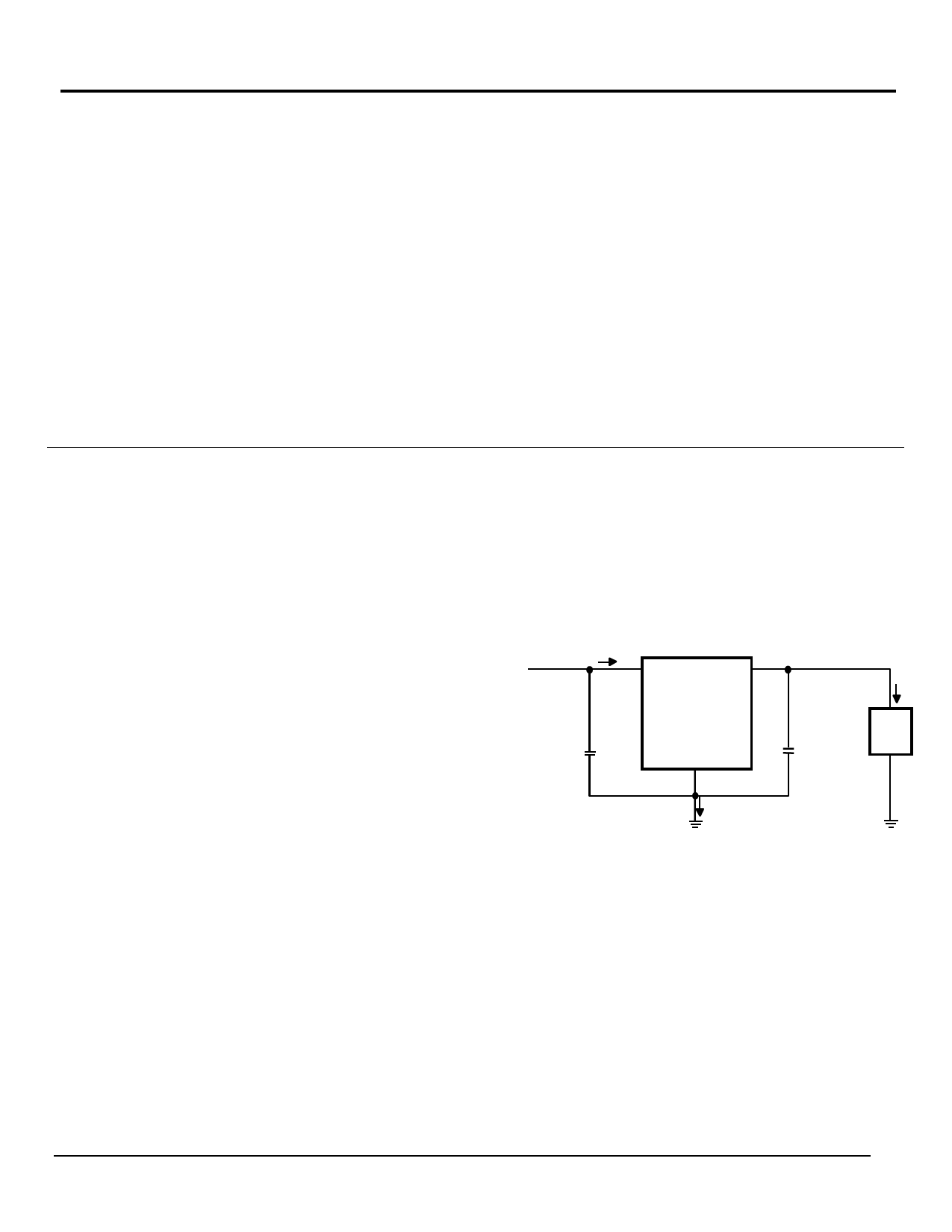
VOUT
IIN
IN
5V
OUT
SPX1129
+
GND
+
2.2uF
IIN = IL + IG
IG
Figure 3. Fixed +5V Regulator Circuit
IL
LOAD
Rev. 10/25/00
Share Link: 