SPT7863 Просмотр технического описания (PDF) - Cadeka Microcircuits LLC.
Номер в каталоге
Компоненты Описание
производитель
SPT7863 Datasheet PDF : 11 Pages
| |||

CLOCK INPUT
DIGITAL OUTPUTS
The SPT7863 is driven from a single-ended TTL-input
clock. Because of the aggressive design of the SPT7863,
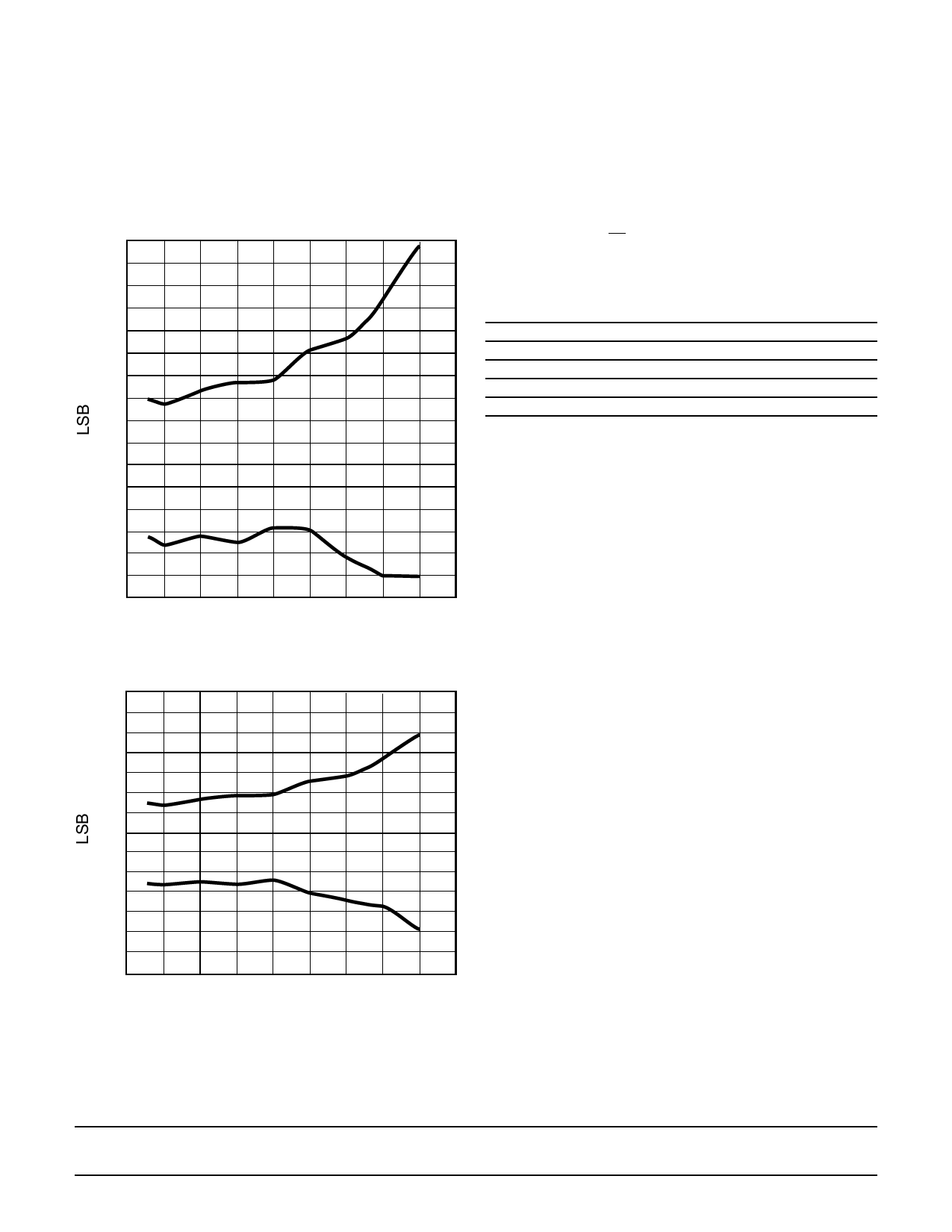
its clock duty cycle ranges from 40% to 51% (see figure 7
– DLE vs Clock Duty Cycle). Operation beyond 51% duty
cycle may result in missing codes.
Figure 7 – DLE vs Clock Duty Cycle
2.0
1.8
1.6
1.4
1.2
1.0
0.8
0.6
0.4
0.2
0.0
0.2
0.4
0.6
0.8
1.0
1.2
38 40 42 44 46 48 50 52 54 56
Clock Duty Cycle (%)
Figure 8 – ILE vs Clock Duty Cycle
2.8
2.4
2.0
1.6
1.2
0.8
0.4
0.0
0.4
0.8
1.2
1.6
2.0
2.4
2.8
38 40 42 44 46 48 50 52 54 56
Clock Duty Cycle (%)
The digital outputs (D0–D10) are driven by a separate
supply (OVDD) ranging from +3 V to +5 V. This feature
makes it possible to drive the SPT7863’s TTL/CMOS-
compatible outputs with the user’s logic system supply.
The format of the output data (D0–D9) is straight binary.
(See table III.) The outputs are latched on the rising edge
of CLK. These outputs can be switched into a tri-state
mode by bringing EN high.
Table III – Output Data Information
ANALOG INPUT OVERRANGE OUTPUT CODE
D10
D9–D0
+F.S. + 1/2 LSB
1
11 1111 1111
+F.S. –1/2 LSB
0
1 1 1 1 1 1 1 1 1Ø
+1/2 F.S.
0
ØØ ØØØØ ØØØØ
+1/2 LSB
0
00 0000 000Ø
0.0 V
0
00 0000 0000
(Ø indicates the flickering bit between logic 0 and 1.)
OVERRANGE OUTPUT
The OVERRANGE OUTPUT (D10) is an indication that
the analog input signal has exceeded the positive full-
scale input voltage by 1 LSB. When this condition occurs,
D10 will switch to logic 1. All other data outputs (D0 to D9)
will remain at logic 1 as long as D10 remains at logic 1.
This feature makes it possible to include the SPT7863 in
higher resolution systems.
EVALUATION BOARD
The EB7863 evaluation board is available to aid designers
in demonstrating the full performance of the SPT7863.
This board includes a reference circuit, clock driver circuit,
output data latches, and an on-board reconstruction of the
digital data. An application note describing the operation
of this board, as well as information on the testing of the
SPT7863, is also available. Contact the factory for price
and availability.
SPT7863
9
8/21/01