UDA1342TS Просмотр технического описания (PDF) - Philips Electronics
Номер в каталоге
Компоненты Описание
производитель
UDA1342TS Datasheet PDF : 44 Pages
| |||
Philips Semiconductors
Audio CODEC
Preliminary specification
UDA1342TS
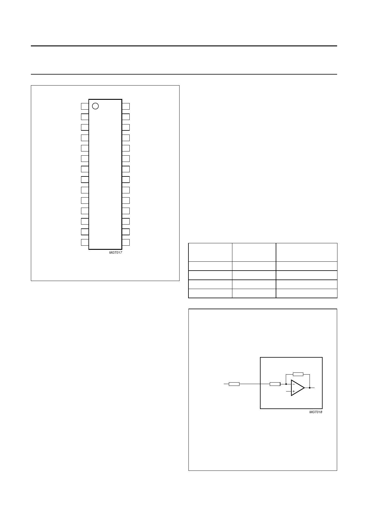
handbook, halfpage
VSSA(ADC) 1
VINL1 2
28 Vref
27 VSSA(DAC)
VDDA(ADC) 3
26 VOUTL
VINR1 4
25 VDDA(DAC)
VADCN 5
24 VOUTR
VINL2 6
23 QMUTE
VADCP 7
22 STATUS
UDA1342TS
VINR2 8
21 STATIC
IPSEL 9
VDDD 10
VSSD 11
SYSCLK 12
20 TEST1
19 DATAI
18 DATAO
17 WS
L3MODE 13
16 BCK
L3CLOCK 14
15 L3DATA
MGT017
Fig.2 Pin configuration.
8 FUNCTIONAL DESCRIPTION
8.1 System clock
The UDA1342TS operates in slave mode only, this means
that in all applications the system must provide the system
clock. The system clock frequency is selectable and
depends on the mode of operation:
• L3-bus/I2C-bus mode: 256fs, 384fs, 512fs or 768fs
• Static pin mode: 256fs or 384fs.
The system clock must be locked in frequency to the digital
interface signals.
Remarks:
• The bit clock frequency fBCK can be up to 128fs, or in
other words the bit clock frequency is 128 times the
word select frequency fWS or less: fBCK ≤ 128fWS
• The WS edge MUST fall on the negative edge of the
BCK signal at all times for proper operation of the digital
interface
• The UDA1342TS operates with sample frequencies
from 16 to 110 kHz, however for a system clock of 768fs
the sampling frequency must be limited to 55 kHz.
8.2 ADC analog front-end
The analog front-end of the UDA1342TS consists of two
stereo ADCs with a programmable gain stage (gain from
0 to 24 dB with 3 dB steps) which can be controlled via the
L3-bus/I2C-bus interface.
8.2.1 APPLICATION WITH 2 V (RMS) INPUT
In applications in which a 2 V (RMS) input signal is used,
a 15 kΩ resistor must be used in series with the input of the
ADC (see Fig.3). This forms a voltage divider together with
the internal ADC resistor and ensures that only 1 V (RMS)
maximum is input to the IC. Using this application for a
2 V (RMS) input signal, the gain switch must be set to
0 dB. When a 1 V (RMS) input signal is input to the ADC in
the same application, the gain switch must be set to 6 dB.
An overview of the maximum input voltages allowed
against the presence of an external resistor and the setting
of the gain switch is given in Table 1.
Table 1 Application modes using input gain stage
RESISTOR
(15 kΩ)
Present
Present
Absent
Absent
PGA GAIN
0 dB
6 dB
0 dB
6 dB
MAXIMUM INPUT
VOLTAGE
2 V (RMS)
1 V (RMS)
1 V (RMS)
0.5 V (RMS)
handbook, halfpage
input signal
2 V (RMS)
15 kΩ
VINL1, 2,
VINR1, 4,
VINL2, 6,
VINR2 8 10 kΩ
gain = 0 dB
10 kΩ
Vref
UDA1342TS
MGT018
Fig.3 Schematic of ADC front-end.
2000 Mar 29
8
Share Link: 