UDA1342TS Просмотр технического описания (PDF) - Philips Electronics
Номер в каталоге
Компоненты Описание
производитель
UDA1342TS Datasheet PDF : 44 Pages
| |||
Philips Semiconductors
Audio CODEC
Preliminary specification
UDA1342TS
8.15.4 DATA WRITE MODE
The data write format is given in Table 13 and illustrated
in Fig.9.
When writing data to a device four bytes must be sent:
1. One byte with the device address, being ‘01X0 1000’
where ‘X’ stands for the IPSEL value, including ‘01’ for
signalling write to the device.
2. One byte starting with a logic 0 for signalling write
followed by 7 bits indicating the register address.
3. One byte which is the Most Significant Data (MSD)
byte 1.
4. One byte which is the Least Significant Data (LSD)
byte 2.
8.15.5 DATA READ MODE
The data write format is given in Table 14 and illustrated
in Fig.10.
When reading from the device, a prepare read must first be
done. After the prepare read, the device address is sent
again. The device then returns with the register address,
indicating whether the address was valid or not, and the
data of the register.
The data read mode is explained below:
1. One byte with the device address, being ‘01X0 1000’
where ‘X’ stands for the IPSEL value, including ‘01’ for
signalling write to the device.
2. One byte is sent with the register address which needs
to be read. This byte starts with a logic 1, which
indicates that there will be a read action from the
register.
3. One byte with the device address including ‘11’ is sent
to the device. The ‘11’ indicates that the device must
write data to the microcontroller.
4. The device now writes the requested register address
on the L3-bus, indicating whether the requested
register was valid (logic 0) or invalid (logic 1).
5. The device writes data from the requested register to
the L3-bus with the MSD byte 1 first, followed by the
LSD byte 2.
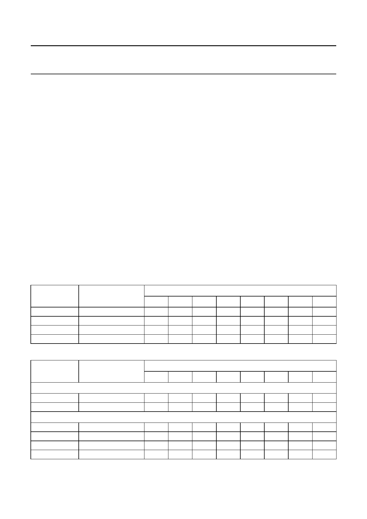
Table 13 L3-bus format for data write
L3MODE
DATA TYPE
Address
Data transfer 1
Data transfer 2
Data transfer 3
device address
register address
MSD byte 1
LSD byte 2
FIRST IN TIME
BIT 0
0
0
D15
D7
BIT 1
1
A6
D14
D6
BIT 2
IPSEL
A5
D13
D5
BIT 3
0
A4
D12
D4
BIT 4
1
A3
D11
D3
BIT 5
0
A2
D10
D2
LAST IN TIME
BIT 6
0
A1
D9
D1
BIT 7
0
A0
D8
D0
Table 14 L3-bus format for prepare read and read data
L3MODE
DATA TYPE
FIRST IN TIME
BIT 0 BIT 1
Prepare read
Address
Data transfer 1
Read data
Address
Data transfer 1
Data transfer 2
Data transfer 3
device address
register address
device address
register address
MSD byte 1
LSD byte 2
0
1
1
A6
1
1
0/1
A6
D15 D14
D7
D6
BIT 2
IPSEL
A5
IPSEL
A5
D13
D5
BIT 3
0
A4
0
A4
D12
D4
BIT 4
1
A3
1
A3
D11
D3
BIT 5
0
A2
0
A2
D10
D2
LAST IN TIME
BIT 6 BIT 7
0
0
A1
A0
0
0
A1
A0
D9
D8
D1
D0
2000 Mar 29
16
Share Link: 