SN74LS259 Просмотр технического описания (PDF) - ON Semiconductor
Номер в каталоге
Компоненты Описание
производитель
SN74LS259 Datasheet PDF : 8 Pages
| |||
ED
14
13
SN74LS259
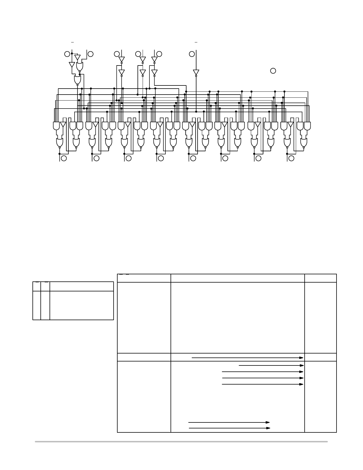
LOGIC DIAGRAM
A0
A1 A2
C
1
2
3
15
VCC = PIN 16
GND = PIN 8
= PIN NUMBERS
4
5
6
7
Q0
Q1
Q2
Q3
FUNCTIONAL DESCRIPTION
The SN74LS259 has four modes of operation as shown in
the mode selection table. In the addressable latch mode, data
on the Data line (D) is written into the addressed latch.The
addressed latch will follow the data input with all
non-addressed latches remaining in their previous states. In
the memory mode, all latches remain in their previous state
and are unaffected by the Data or Address inputs.
In the one-of-eight decoding or demultiplexing mode, the
addressed output will follow the state of the D input with all
9
10
11
12
Q4
Q5
Q6
Q7
other inputs in the LOW state. In the clear mode all outputs
are LOW and unaffected by the address and data inputs.
When operating the SN74LS259 as an addressable latch,
changing more then one bit of the address could impose a
transient wrong address. Therefore, this should only be done
while in the memory mode.
The truth table below summarizes the operations.
MODE SELECTION
EC
MODE
LH
HH
LL
HL
Addressable Latch
Memory
Active HIGH Eight-Channel
Demultiplexer
Clear
X = Don’t Care Condition
L = LOW Voltage Level
H = HIGH Voltage Level
QN–1 = Previous Output State
TRUTH TABLE
PRESENT OUTPUT STATES
C E D A0 A1 A2 Q0 Q1 Q2 Q3 Q4 Q5 Q6 Q7
MODE
L HX X X X L
L
L
L
L
L
L
L Clear
LLL L L L L
L
L
L
L
L
L
L Demultiplex
LLH L L L H
L
L
L
L
L
L
L
LLL H L L L
L
L
L
L
L
L
L
LLH H L L L
H
L
L
L
L
L
L
•••
•
•
•••
•
•
•••
•
•
•••
•
•
•••
•
•
LLH H H H L
L
L
L
L
L
L
H
H H X X X X QN–1
HI I L L L
L QN–1 QN–1 QN–1
H L H L L L H QN–1 QN–1
H L L H L L QN–1 L QN–1
H L H H L L QN–1 H QN–1
•••
•
•
•••
•
•
•••
•
•
•••
•
•
•••
•
•
H L L H H H QN–1
H L H H H H QN–1
Memory
Addressable
Latch
QN–1 L
QN–1 H
http://onsemi.com
3
Share Link: 