ML4661CS Просмотр технического описания (PDF) - Micro Linear Corporation
Номер в каталоге
Компоненты Описание
производитель
ML4661CS Datasheet PDF : 8 Pages
| |||
FUNCTIONAL DESCRIPTION
The ML4761 combines Pulse Frequency Modulation
(PFM) and synchronous rectification to create a boost
converter that is both highly efficient and simple to use.
A PFM regulator charges a single inductor for a fixed
period of time and then completely discharges before
another cycle begins, simplifying the design by
eliminating the need for conventional current limiting
circuitry. Synchronous rectification is accomplished by
replacing an external Schottky diode with an on-chip
PMOS device, reducing switching losses and external
component count.
REGULATOR OPERATION
A block diagram of the boost converter is shown in Figure
2. The circuit remains idle when VOUT is at or above the
desired output voltage, drawing 45µA from VIN, and 8µA
from VOUT through the feedback resistors R1 and R2.
When VOUT drops below the desired output level, the
output of amplifier A1 goes high, signaling the regulator to
deliver charge to the output. Since the output of amplifier
A2 is normally high, the flip-flop captures the A1 set signal
and creates a pulse at the gate of the NMOS transistor Q1.
The NMOS transistor will charge the inductor L1 for 10µs,
resulting in a peak current given by:
IL(PEAK)
=
TON × VIN
L1
≈
10µs × VIN
L1
(1)
For reliable operation, L1 should be chosen so that IL(PEAK)
does not exceed 2A.
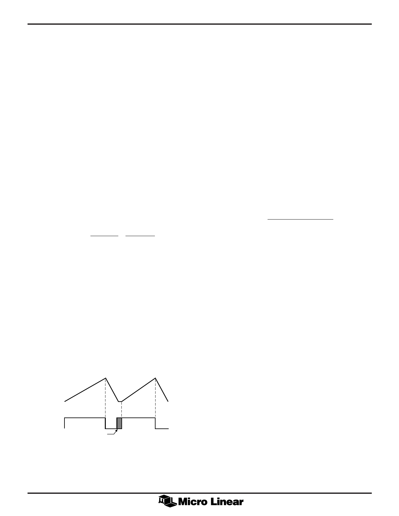
When the one-shot times out, the NMOS FET releases the
VL pin, allowing the inductor to fly-back and momentarily
charge the output through the body diode of PMOS
transistor Q2. But, as the voltage across the PMOS
transistor changes polarity, its gate will be driven low by
the current sense amplifier A2, causing Q2 to short out its
body diode. The inductor then discharges into the load
through Q2. The output of A2 also serves to reset the flip-
flop and one-shot in preparation for the next charging
cycle. A2 releases the gate of Q2 when its current falls to
zero. If VOUT is still low, the flip-flop will immediately
initiate another pulse. The output capacitor (C1) filters the
inductor current, limiting output voltage ripple. Inductor
current and one-shot waveforms are shown in Figure 3.
ML4761
RESET COMPARATOR
An additional comparator is provided to detect low VIN.
The inverting input of the comparator is internally
connected to VREF, while the non-inverting input is
connected to the undervoltage lockout circuit. The output
of the comparator is the RESET pin, which swings from
VOUT to GND when an undervoltage condition is
detected.
DESIGN CONSIDERATIONS
INDUCTOR
Selecting the proper inductor for a specific application
usually involves a trade-off between efficiency and
maximum output current. Choosing too high a value will
keep the regulator from delivering the required output
current under worst case conditions. Choosing too low a
value causes efficiency to suffer. It is necessary to know
the maximum required output current and the input
voltage range to select the proper inductor value. The
maximum inductor value can be estimated using the
following formula:
LMAX
=
VIN(MIN)2 × TON(MIN) × η
2 × VOUT × IOUT(MAX)
(2)
where h is the efficiency, typically between 0.8 and 0.9.
Note that this is the value of inductance that just barely
delivers the required output current under worst case
conditions. A lower value may be required to cover
inductor tolerance, the effect of lower peak inductor
currents caused by resistive losses, and minimum dead
time between pulses.
Another method of determining the appropriate inductor
value is to make an estimate based on the typical
performance curves given in Figures 4 and 5. Figure 4
shows maximum output current as a function of input
voltage for several inductor values. These are typical
performance curves and leave no margin for inductance
and ON-time variations. To accommodate worst case
conditions, it is necessary to derate these curves by at
least 10% in addition to inductor tolerance. Interpolation
between the different curves will give a reasonable
starting point for an inductor value.
INDUCTOR
CURRENT
Q(ONE SHOT)
Q2
Q1 ON
ON
Q1 & Q2 OFF
Q2
Q1 ON
ON
Figure 3. PFM Inductor Current Waveforms and Timing.
5
Share Link: 