SMJ44400 Просмотр технического описания (PDF) - Austin Semiconductor
Номер в каталоге
Компоненты Описание
производитель
SMJ44400 Datasheet PDF : 21 Pages
| |||
Austin Semiconductor, Inc.
DRAM
SMJ44400
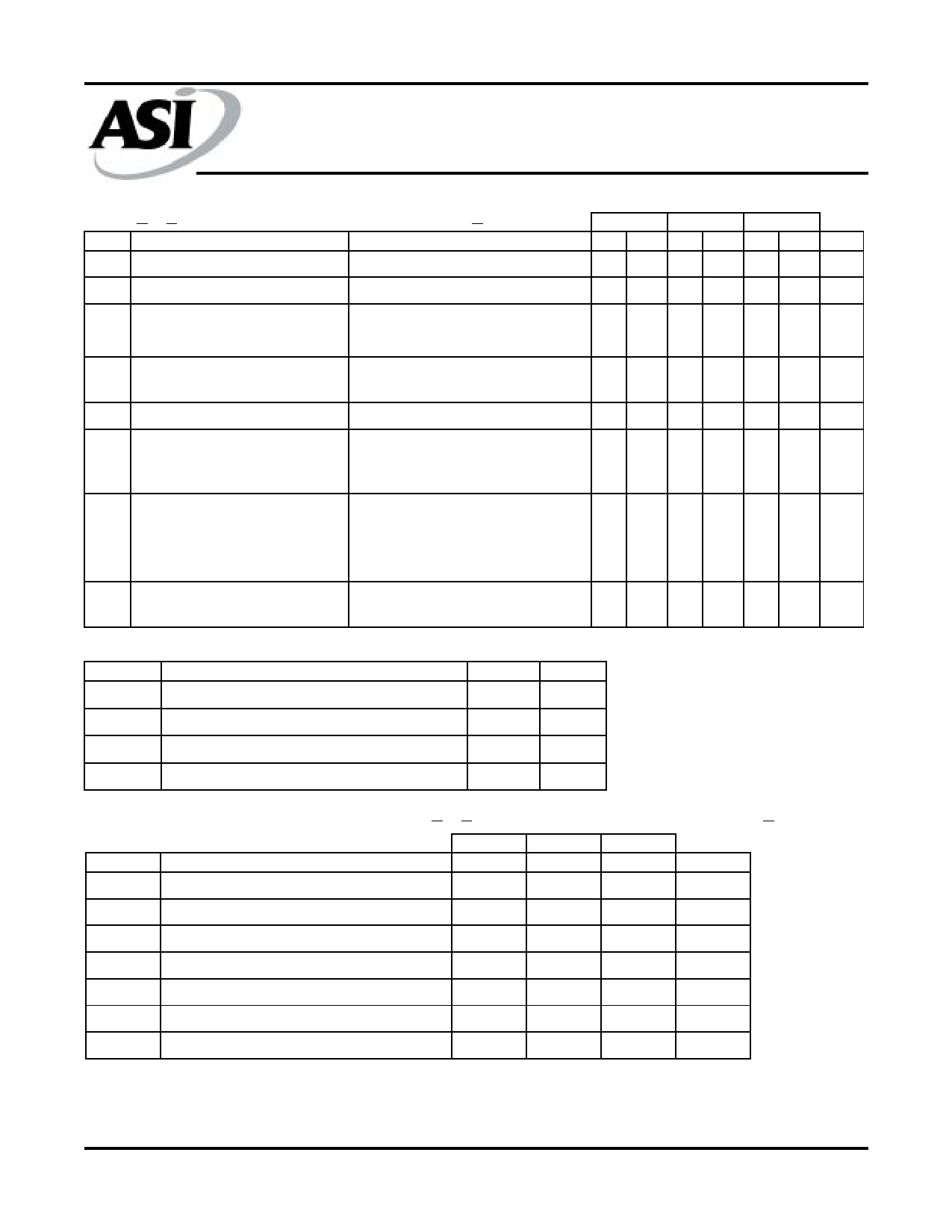
ELECTRICAL CHARACTERISTICS AND RECOMMENDED OPERATING CONDITIONS
(-55oC<TA<125oC or -40oC to +85oC; Vcc = 5V +10%)
SYM
PARAMETER
TEST CONDITIONS
-8
-10
-12
MIN MAX MIN MAX MIN MAX UNIT
VOH High-level output voltage
IOH = -5mA
2.4
2.4
2.4
V
VOL Low-level output voltage
IOL = 4.2mA
0.4
0.4
0.4 V
II Input current (leakage)
IO Output current (leakage)
ICC1 Read - or write-cycle current1
ICC2 Standby current
VCC = 5.5V, VI = 0V to 6.5V, All
other pins = 0V to VCC
VCC = 5.5V, VO = 0V to VCC,
CAS\ High
VCC = 5.5V, Minimum cycle
After 1 memory cycle,
RAS\ and CAS\ High,
VIH = 2.4V
±10
±10
±10 µA
±10
±10
±10 µA
85
80
70 mA
4
4
4 mA
Average refresh current
ICC3 (RAS\ only, or CBR\)1
VCC = 5.5V, Minimum cycle,
RAS\ cycling,
CAS\ High (RAS\ only),
RAS\ Low after CAS\ Low (CBR)
85
75
65 mA
ICC4 Average page current2
VCC = 5.5V, tPC = minimum,
RAS\ Low, CAS\ cycling
50
40
35 mA
CAPACITANCE (f = 1MHz)3
SYM
Ci(A)
Ci(RC)
Ci(W)
CO
PARAMETER
Input capacitance, address inputs
Input capacitance, strobe inputs
Input capacitance, write-enable inputs
Output capacitance
MAX
7
10
10
10
UNIT
pF
pF
pF
pF
SWITCHING CHARACTERISTICS (-55oC<TA<125oC or -40oC to +85oC; Vcc = 5V +10%)
SYM
PARAMETERS
-8
MAX
-10
MAX
-12
MAX
UNIT
tAA Access time from column address
40
45
55
ns
tCAC Access time from CAS\ low
20
25
30
ns
tCPA Access time from column precharge
45
50
55
ns
tRAC Access time from RAS\ low
80
100
120
ns
tOEA Access time from OE\ low
20
25
30
ns
tOFF Output disable time after CAS\ High4
20
25
30
ns
tOEZ Output disable tiem after OE\ High4
20
25
30
ns
NOTES:
1. Measured with a maximum of one address change while RAS\ = VIL.
2. Measured with a maximum of one address change while CAS\ = VIH.
3. VCC = 5V ±0.5V and the bias on the pins under test is 0V. Capacitance is sampled only at initial design and after any major change.
4. tOFF and tOEZ are specified when the output is no longer driven. The outputs are disabled by bringing either OE\ or CAS\ High.
SMJ44400
Rev. 2.0 10/01
Austin Semiconductor, Inc. reserves the right to change products or specifications without notice.
5
Share Link: 