SL74HC112N Просмотр технического описания (PDF) - System Logic Semiconductor
Номер в каталоге
Компоненты Описание
производитель
SL74HC112N
System Logic Semiconductor

SL74HC112N Datasheet PDF : 6 Pages
| |||
SL74HC112
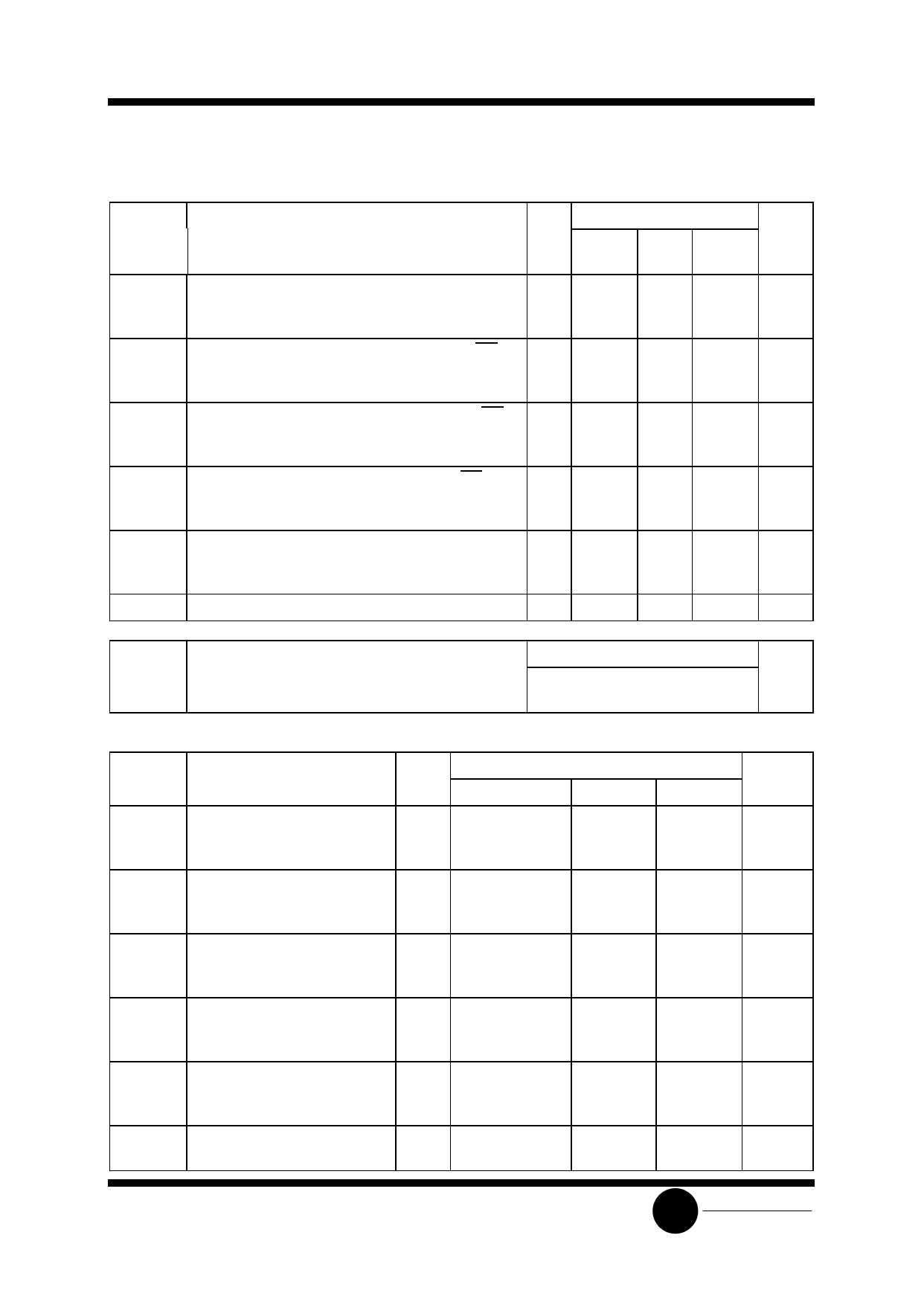
AC ELECTRICAL CHARACTERISTICS(CL=50pF,Input tr=tf=6.0 ns)
Symbol
Parameter
fmax Maximum Clock Frequency (50% Duty Cycle)
(Figures 1 and 4)
tPLH, tPHL Maximum Propagation Delay, Clock to Q or Q
(Figures 1 and 4)
tPLH, tPHL Maximum Propagation Delay , Reset to Q or Q
(Figures 2 and 4)
tPLH, tPHL Maximum Propagation Delay ,Set to Q or Q (Figures
2 and 4)
tTLH, tTHL Maximum Output Transition Time, Any Output
(Figures 1 and 4)
CIN
Maximum Input Capacitance
VCC
Guaranteed Limit
V 25 °C to ≤85°C ≤125°C
-55°C
2.0 6.0
4.8
4.0
4.5 30
24
20
6.0 35
28
24
2.0 125 155 190
4.5 25
31
38
6.0 21
26
32
2.0 155 195 235
4.5 31
39
47
6.0 26
33
40
2.0 165 205 250
4.5 33
41
50
6.0 28
35
43
2.0 75
4.5 15
6.0 13
95
110
19
22
16
19
-
10
10
10
Unit
MHz
ns
ns
ns
ns
pF
Power Dissipation Capacitance (Per Flip-Flop)
Typical @25°C,VCC=5.0 V
CPD Used to determine the no-load dynamic power
consumption: PD=CPDVCC2f+ICCVCC
35
pF
TIMING REQUIREMENTS (CL=50pF,Input tr=tf=6.0 ns)
VCC
Symbol
Parameter
V
tSU
Minimum Setup Time,J or K to 2.0
Clock (Figure 3)
4.5
6.0
th
Minimum Hold Time, Clock to 2.0
J or K (Figure 3)
4.5
6.0
trec
Minimum Recovery Time, Set
2.0
or Reset Inactive to Clock
4.5
(Figure 2)
6.0
tw
Minimum Pulse Width, Clock
2.0
(Figure 1)
4.5
6.0
tw
Minimum Pulse Width, Set or
2.0
Reset (Figure 2)
4.5
6.0
tr, tf Maximum Input Rise and Fall
2.0
Times (Figure 1)
4.5
6.0
Guaranteed Limit
25 °C to-55°C
≤85°C
≤125°C
Unit
100
125
150
ns
20
25
30
17
21
26
3
3
3
ns
3
3
3
3
3
3
100
125
150
ns
20
25
30
17
21
26
80
100
120
ns
16
20
24
14
17
20
80
100
120
ns
16
20
24
14
17
20
1000
1000
1000
ns
500
500
500
400
400
400
SLS
System Logic
Semiconductor
Share Link: