IRFP22N50A Просмотр технического описания (PDF) - Vishay Semiconductors
Номер в каталоге
Компоненты Описание
производитель
IRFP22N50A Datasheet PDF : 8 Pages
| |||
IRFP22N50A, SiHFP22N50A
Vishay Siliconix
THERMAL RESISTANCE RATINGS
PARAMETER
SYMBOL
Maximum Junction-to-Ambient
Case-to-Sink, Flat, Greased Surface
RthJA
RthCS
Maximum Junction-to-Case (Drain)
RthJC
TYP.
-
0.24
-
MAX.
40
-
0.45
UNIT
°C/W
SPECIFICATIONS TJ = 25 °C, unless otherwise noted
PARAMETER
SYMBOL
TEST CONDITIONS
MIN. TYP. MAX. UNIT
Static
Drain-Source Breakdown Voltage
VDS Temperature Coefficient
Gate-Source Threshold Voltage
Gate-Source Leakage
Zero Gate Voltage Drain Current
Drain-Source On-State Resistance
Forward Transconductance
Dynamic
VDS
ΔVDS/TJ
VGS(th)
IGSS
IDSS
RDS(on)
gfs
VGS = 0 V, ID = 250 µA
Reference to 25 °C, ID = 1 mA
VDS = VGS, ID = 250 µA
VGS = ± 30 V
VDS = 500 V, VGS = 0 V
VDS = 400 V, VGS = 0 V, TJ = 125 °C
VGS = 10 V
ID = 13 Ab
VDS = 50 V, ID = 13 Ab
500
-
-
V
-
0.55
-
V/°C
2.0
-
4.0
V
-
-
± 100 nA
-
-
25
µA
-
-
250
-
-
0.23
Ω
12
-
-
S
Input Capacitance
Ciss
Output Capacitance
Coss
Reverse Transfer Capacitance
Crss
Output Capacitance
Coss
Effective Output Capacitance
Total Gate Charge
Gate-Source Charge
Gate-Drain Charge
Turn-On Delay Time
Rise Time
Turn-Off Delay Time
Fall Time
Drain-Source Body Diode Characteristics
Coss eff.
Qg
Qgs
Qgd
td(on)
tr
td(off)
tf
Continuous Source-Drain Diode Current
IS
Pulsed Diode Forward Currenta
ISM
-
VGS = 0 V,
VDS = 25 V,
-
f = 1.0 MHz, see fig. 5
-
VDS = 1.0 V, f = 1.0 MHz
VGS = 0 V VDS = 400 V, f = 1.0 MHz
VDS = 0 V to 400 Vc
-
VGS = 10 V
ID = 22 A, VDS = 400 V,
see fig. 6 and 13b
-
-
-
VDD = 250 V, ID = 22 A,
-
RG = 4.3 Ω, RD = 11 Ω, see fig. 10b
-
-
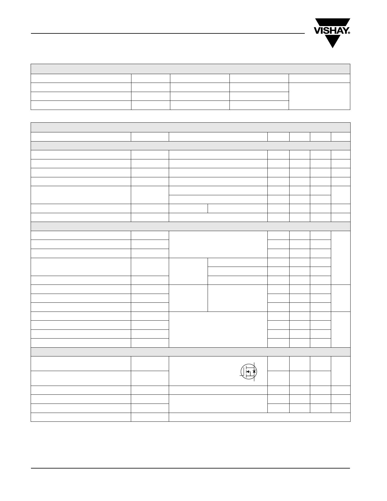
MOSFET symbol
showing the
D
-
integral reverse
G
p - n junction diode
-
S
3450
-
513
-
27
-
pF
4935
137
264
-
120
-
32
nC
-
52
26
-
94
-
ns
47
-
47
-
-
22
A
-
88
Body Diode Voltage
VSD
TJ = 25 °C, IS = 22A, VGS = 0 Vb
-
-
1.5
V
Body Diode Reverse Recovery Time
Body Diode Reverse Recovery Charge
trr
-
570
850
ns
TJ = 25 °C, IF = 22 A, dI/dt = 100 A/µsb
Qrr
-
6.1
9.2
µC
Forward Turn-On Time
ton
Intrinsic turn-on time is negligible (turn-on is dominated by LS and LD)
Notes
a. Repetitive rating; pulse width limited by maximum junction temperature (see fig. 11).
b. Pulse width ≤ 300 µs; duty cycle ≤ 2 %.
c. Coss eff. is a fixed capacitance that gives the same charging time as Coss while VDS is rising from 0 to 80 % VDS.
www.vishay.com
2
Document Number: 91207
S-81264-Rev. A, 21-Jul-08
Share Link: 