SI9988 Просмотр технического описания (PDF) - Vishay Semiconductors
Номер в каталоге
Компоненты Описание
производитель
SI9988 Datasheet PDF : 7 Pages
| |||
Si9988
Vishay Siliconix
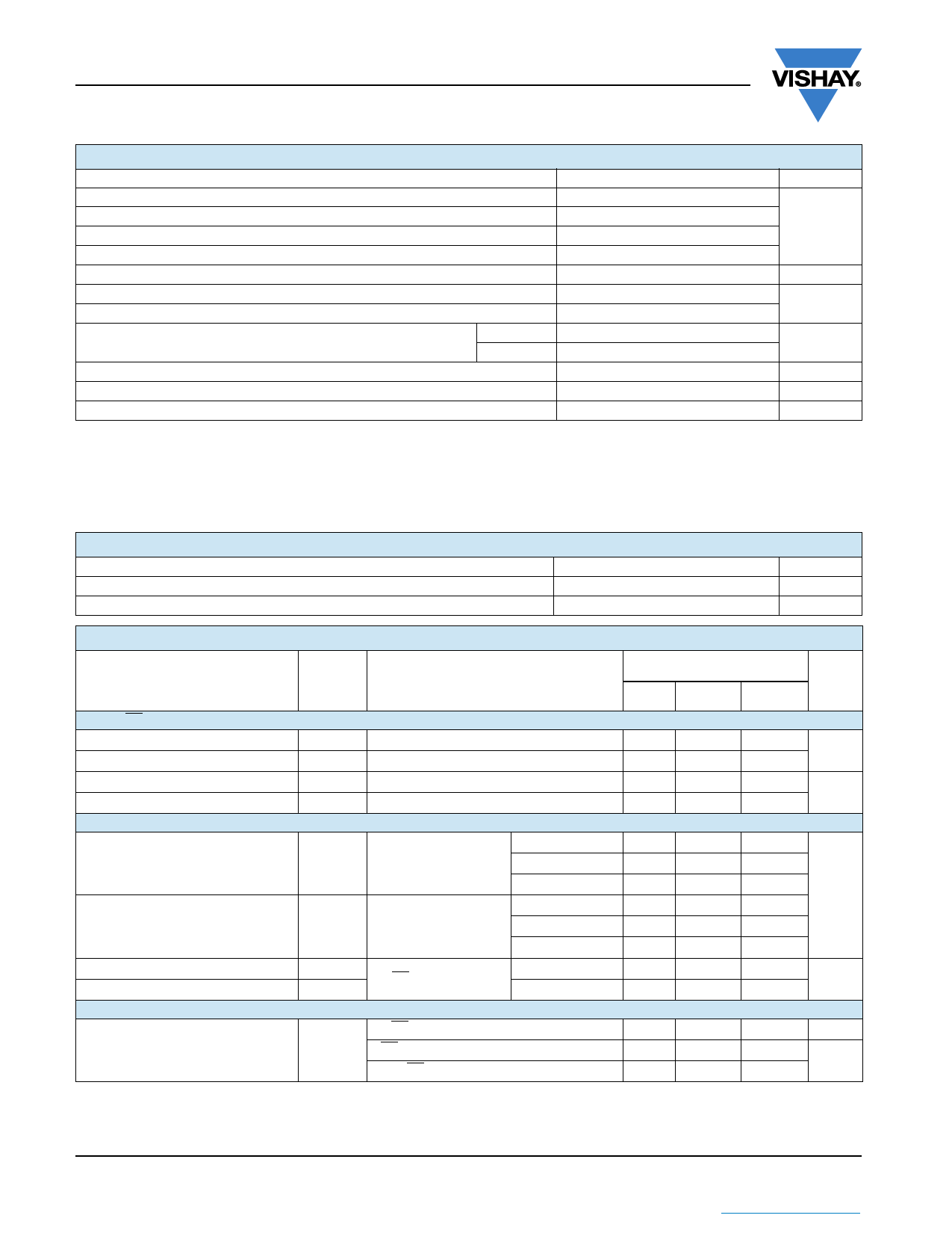
ABSOLUTE MAXIMUM RATINGSa
Parameter
Limit
Unit
VDD
Voltage on any Pin with Respect to Ground
Voltage on Pins 5, 8 with Respect to Ground
Voltage on Pins 6, 7
15
- 0.3 to VDD + 0.3
V
- 1 to VDD + 1
- 0.3 to GND + 1
Peak Output Current
1
A
Storage Temperature
Junction Temperature (TJ)
- 65 to 150
°C
150
Continuos Iout Current (TJ = 135 °C, YDD = 5 V)
TA = 25 °C
TA = 85 °C
0.67
0.47
A
Power Dissipationb
0.83
W
θJA
120
°C/W
Operating Temperature Range
- 40 to 85
°C
Notes:
a. Device mounted with all leads soldered or welded to PC board.
b. Derate 8.3 mW/°C above 25 °C.
c. TJ = TA + (PD)(θJA), PD = power dissipation.
Stresses beyond those listed under “Absolute Maximum Ratings” may cause permanent damage to the device. These are stress ratings only, and functional operation
of the device at these or any other conditions beyond those indicated in the operational sections of the specifications is not implied. Exposure to absolute maximum
rating conditions for extended periods may affect device reliability.
RECOMMENDED OPERATING RANGE
Parameter
VDD
Maximum Junction Temperature (TJ)
SPECIFICATIONS
Parameter
Symbol
Input (EN, PWM)
Input Voltage High
Input Voltage Low
Input Current with Input Voltage High
Input Current with Input Voltage Low
Output
VINH
VINL
IINH
IINL
Output Voltage Highc
VOUTH
Output Voltage Lowc
Output V Clamp High
Output V Clamp Low
Supply
VDD Supply Current
VOUTL
VCLH
VCLL
IDD
Test Conditions
Unless Otherwise Specified
VDD = 3.8 to 13.2 V
SA at GND, SB at GND
VIN = 13.2 V
VIN = 0 V
IOUT = - 300 mA
IOUT = 300 mA
EN = PWM ≥ 2 V
VDD = 10.8 V
VDD = 4.5 V
VDD = 3.8 V
VDD = 10.8 V
VDD = 4.5 V
VDD = 3.8 V
IOUT = 100 mA
IOUT = - 100 mA
EN = 0 V, PWM = 100 kHz, VDD = 5 V
EN = 4.5 V, PWM = 100 kHz, VDD = 5.5 V
EN = PWM = 4.5 V, VDD = 5.5 V
Limit
Unit
3.8 to 13.2
V
135
°C
Limits
D Suffix, - 40 °C to 85 °C
Unit
Mina
Typb
Maxa
2
V
1
1
µA
-1
10.55 10.70
4.20
4.35
3.40
3.62
V
0.09
0.20
0.12
0.25
0.14
0.30
VDD + 0.7 VDD + 1.0
V
- 1.0
- 0.7
1.0
1.5
mA
60
140
µA
55
110
www.vishay.com
Document Number: 71326
2
S11-0800-Rev. C, 25-Apr-11
This document is subject to change without notice.
THE PRODUCTS DESCRIBED HEREIN AND THIS DOCUMENT ARE SUBJECT TO SPECIFIC DISCLAIMERS, SET FORTH AT www.vishay.com/doc?91000
Share Link: 