SI5317 Просмотр технического описания (PDF) - Silicon Laboratories
Номер в каталоге
Компоненты Описание
производитель
SI5317 Datasheet PDF : 50 Pages
| |||

Si5317
PRELIMINARY DATA SHEET
PIN-CONTROLLED 1–710 MHZ JITTER CLEANING CLOCK
Features
Provides jitter attenuation on any
frequency
One clock input / two clock outputs
Input/output frequency range:
1–710 MHz
Ultra low jitter: 300 fs
(12 kHz–20 MHz) typical
Simple pin control interface
Selectable loop bandwidth for jitter
attenuation: 60 Hz–8.4 kHz
Applications
Data converter clocking
Wireless infrastructure
Networking, SONET/SDH
Description
Selectable output clock signal
format: LVPECL, LVDS, CML or
CMOS
Single supply: 1.8, 2.5, or 3.3 V
VCO freeze during LOS/LOL
Loss of lock and loss of signal alarms
On-chip voltage regulator with high
PSRR
Small size: 6 x 6 mm, 36-QFN
Wide temperature range: –40 to
+85 ºC
Switches and routers
Medical instrumentation
Test and measurement
The Si5317 is a flexible 1:1 jitter cleaning clock for high-performance applications
that require jitter attenuation without clock multiplication. The Si5317 accepts a
single clock input ranging from 1 to 710 MHz and generates two low jitter clock
outputs at the same frequency. The clock frequency range and loop bandwidth are
selectable from a simple look-up table. The Si5317 is based on Silicon
Laboratories' 3rd-generation DSPLL® technology, which provides jitter attenuation
on any frequency in a highly integrated PLL solution that eliminates the need for
external VCXO and loop filter components. The DSPLL loop bandwidth is user
selectable, providing jitter performance optimization at the application level.
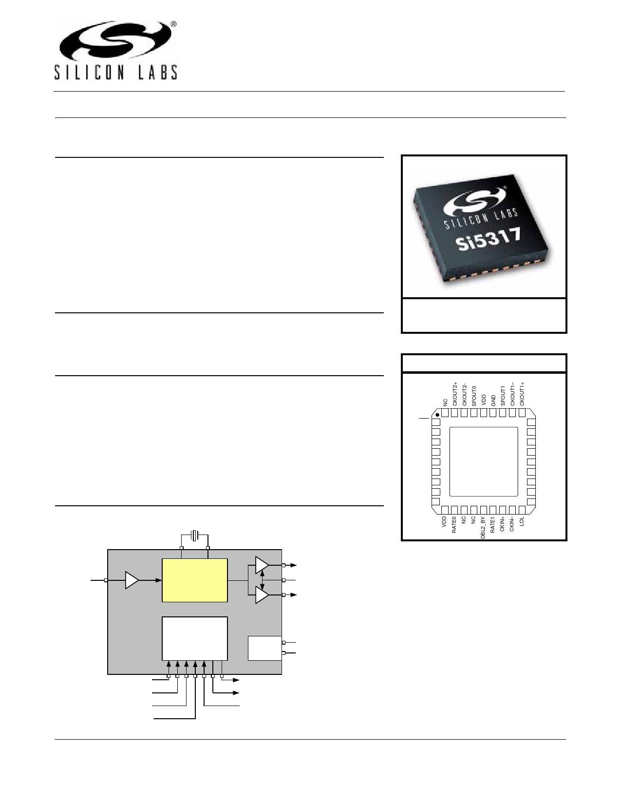
Functional Block Diagram
XTAL/Clock
Ordering Information:
See page 43.
Pin Assignments
36 35 34 33 32 31 30 29 28
RST 1
27 FRQSEL3
FRQTBL 2
26 FRQSEL2
LOS 3
25 FRQSEL1
NC 4
VDD 5
XA 6
GND
Pad
24 FRQSEL0
23 BWSEL1
22 BWSEL0
XB 7
21 NC
GND 8
20 DEC
NC 9
19 INC
10 11 12 13 14 15 16 17 18
Clock In
DSPLL ®
Clock Out1
Signal Format [1:0]
Clock Out2
Status/Control
High
PSRR
Regulator
VDD (1.8, 2.5, 3.3 V)
GND
Frequency Table
Frequency Select [3:0]
Bandwidth Select [1:0]
Phase Skew INC/DEC
Loss of Lock
Loss of Signal
XTAL/Clock Rate [1:0]
Preliminary Rev. 0.15 4/10
Copyright © 2010 by Silicon Laboratories
Si5317
This information applies to a product under development. Its characteristics and specifications are subject to change without notice.