SI5315 Просмотр технического описания (PDF) - Silicon Laboratories
Номер в каталоге
Компоненты Описание
производитель
SI5315 Datasheet PDF : 54 Pages
| |||
Si5315
1. Electrical Specifications
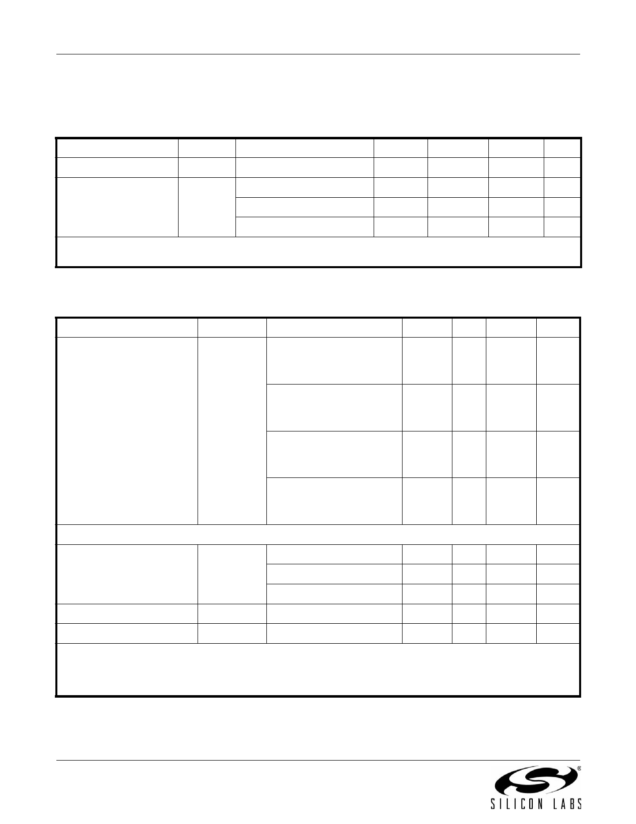
Table 1. Recommended Operating Conditions
(VDD = 1.8 ±5%, 2.5 ±10%, or 3.3 V ±10%, TA = –40 to 85 ºC)
Parameter
Symbol
Test Condition
Min
Typ
Max Unit
Temperature Range
TA
Supply Voltage
VDD
3.3 V nominal
2.5 V nominal
–40
25
85
ºC
2.97
3.3
3.63
V
2.25
2.5
2.75
V
1.8 V nominal
1.71
1.8
1.89
V
Note: All minimum and maximum specifications are guaranteed and apply across the recommended operating conditions.
Typical values apply at nominal supply voltages and an operating temperature of 25 °C unless otherwise noted.
Table 2. DC Characteristics
(VDD = 1.8 ±5%, 2.5 ±10%, or 3.3 V ±10%, TA = –40 to 85 ºC)
Parameter
Symbol
Test Condition
Min Typ Max Units
Supply Current (Supply
current is independent of
VDD)
IDD
LVPECL Format
—
251 279
mA
644.53125 MHz Out
All CKOUTs Enabled1
LVPECL Format
—
217 243
mA
644.53125 MHz Out
Only 1 CKOUT Enabled1
CMOS Format
25.00 MHz Out
All CKOUTs Enabled2
—
204 234
mA
CMOS Format
—
194 220
mA
25.00 MHz Out
Only CKOUT1 Enabled2
CKINn Input Pins
Input Common Mode Voltage
(Input Threshold Voltage)
VICM
1.8 V ± 5%
2.5 V ± 10%
0.9
—
1.4
V
1.0
—
1.7
V
3.3 V ± 10%
1.1
—
1.95
V
Input Resistance
CKNRIN
Single-ended
20
40
60
k
Input Voltage Level Limits
CKNVIN
0
—
VDD
V
Notes:
1. Refers to Si5315A speed grade.
2. Refers to Si5315B speed grade.
3. This is the amount of leakage that the 3L inputs can tolerate from an external driver. See Figure 3 on page 11.
4
Rev. 1.0
Share Link: 