SI4410BDY-T1-GE3(2009) Просмотр технического описания (PDF) - Vishay Semiconductors
Номер в каталоге
Компоненты Описание
производитель
SI4410BDY-T1-GE3 Datasheet PDF : 8 Pages
| |||
Si4410BDY
Vishay Siliconix
SPECIFICATIONS TJ = 25 °C, unless otherwise noted
Parameter
Symbol
Test Conditions
Static
Gate Threshold Voltage
VGS(th)
VDS = VGS, ID = 250 µA
Gate-Body Leakage
IGSS
VDS = 0 V, VGS = ± 20 V
Zero Gate Voltage Drain Current
IDSS
VDS = 30 V, VGS = 0 V
VDS = 30 V, VGS = 0 V, TJ = 55 °C
On-State Drain Currenta
ID(on)
VDS ≥ 5 V, VGS = 10 V
Drain-Source On-State Resistancea RDS(on)
VGS = 10 V, ID = 10 A
VGS = 4.5 V, ID = 5 A
Forward Transconductancea
gfs
VDS = 15 V, ID = 10 A
Diode Forward Voltagea
VSD
IS = 2.3 A, VGS = 0 V
Dynamicb
Gate Charge
Qg
VDS = 15 V, VGS = 5 V, ID = 10 A
Total Gate Charge
Qgt
Gate-Source Charge
Qgs
VDS = 15 V, VGS = 10 V, ID = 10 A
Gate-Drain Charge
Qgd
Gate Resistance
Rg
f = 1 MHz
Turn-On Delay Time
td(on)
Rise Time
Turn-Off Delay Time
tr
td(off)
VDD = 25 V, RL = 25 Ω
ID ≅ 1 A, VGEN = 10 V, Rg = 6 Ω
Fall Time
tf
Source-Drain Reverse Recovery
Time
trr
IF = 2.3 A, dI/dt = 100 A/µs
Notes:
a. Pulse test; pulse width ≤ 300 µs, duty cycle ≤ 2 %.
b. Guaranteed by design, not subject to production testing.
Min.
Typ.
Max.
Unit
1.0
3.0
V
± 100
nA
1
µA
5
20
A
0.011 0.0135
Ω
0.0165 0.020
25
S
0.76
1.1
V
13
20
25
40
nC
5.5
3.7
0.5
1.6
2.7
Ω
10
15
10
15
40
60
ns
15
25
35
70
Stresses beyond those listed under “Absolute Maximum Ratings” may cause permanent damage to the device. These are stress ratings only, and functional operation
of the device at these or any other conditions beyond those indicated in the operational sections of the specifications is not implied. Exposure to absolute maximum
rating conditions for extended periods may affect device reliability.
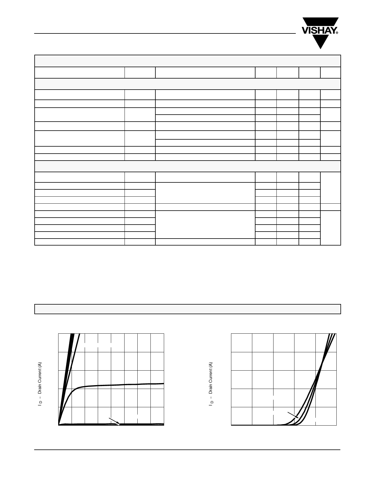
TYPICAL CHARACTERISTICS 25 °C, unless otherwise noted
50
50
VGS = 10 V thru 5 V
40
40
30
30
4V
20
20
10
10
2V
3V
0
0
0.0 0.5 1.0 1.5 2.0 2.5 3.0 3.5 4.0
0
VDS - Drain-to-Source Voltage (V)
Output Characteristics
www.vishay.com
2
TC = 125 °C
25 °C
- 55 °C
1
2
3
4
5
VGS - Gate-to-Source Voltage (V)
Transfer Characteristics
Document Number: 72211
S09-0705-Rev. D, 27-Apr-09
Share Link: 