6742HL Просмотр технического описания (PDF) - Fairchild Semiconductor
Номер в каталоге
Компоненты Описание
производитель
6742HL Datasheet PDF : 13 Pages
| |||
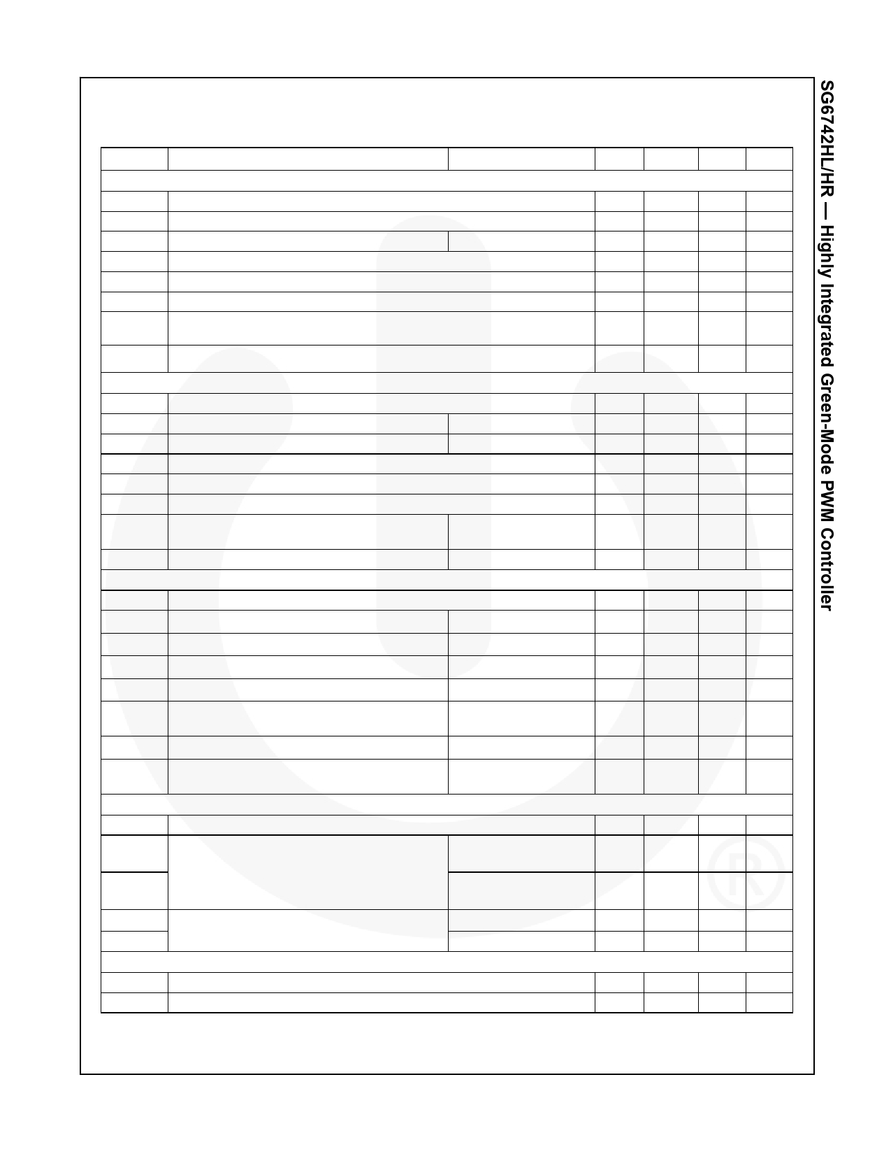
Electrical Characteristics (Continued)
VDD=15V and TA=25°C unless otherwise noted.
Symbol
Parameter
Feedback Input Section
AV
ZFB
VFB-OPEN
VFB-OLP
tD-OLP
VFB-N
Input Voltage to Current-Sense Attenuation
Input Impedance
Output High Voltage
FB Open-Loop Trigger Level
Delay Time of FB Pin Open-loop Protection
Green-Mode Entry FB Voltage
VFB-G Green-Mode Ending FB Voltage
Conditions
FB Pin Open
Min. Typ. Max. Units
1/4.15 1/4.00 1/3.85 V/V
4
7
kΩ
5.2
V
4.6
4.8
5.0
V
50
56
62 ms
3.1
3.3
3.5
V
VFB-N-
0.5
V
VFB-ZDC Zero Duty-Cycle Input Voltage
1.6
V
Current-Sense Section
ZSENSE
VSTHFL
VSTHVA
tPD
tLEB
VS-SCP
tD-SSCP
Input Impedance
Current Limit Flatten Threshold Voltage
Duty cycle=45%
Current Limit Valley Threshold Voltage
VSTHFL–VSTHVA
Delay to Output
Leading-Edge Blanking Time
Threshold Voltage for SENSE Short-Circuit Protection
Delay Time for SENSE Short-Circuit
Protection
VSENSE<0.15V
12
KΩ
0.97 1.00 1.03 V
0.27 0.30 0.33 V
100 200 ns
100 140 180 ns
0.10 0.15 0.20 V
100 150 200 µs
tSS Period During Soft-Startup Time
GATE Section
Startup Time
5
6
7
ms
DCYMAX Maximum Duty Cycle
VGATE-L Gate Low Voltage
VDD=15V, IO=50mA
60
65
70
%
1.5 V
VGATE-H Gate High Voltage
VDD=12V, IO=50mA
8
V
tr
Gate Rising Time
VDD=15V, CL=1nF
150 250 350 ns
tf
Gate Falling Time
IGATE- Gate Source Current
SOURCE
IGATE-SINK Gate Sink Current
VGATE- Gate Output Clamping Voltage
CLAMP
RT Section
VDD=15V, CL=1nF
VDD=15V, GATE=6V
VDD=15V, GATE=1V
VDD=22V
30
50
250
300
90 ns
mA
mA
18
V
RRT Internal Resistor from RT Pin
10.08 10.50 10.92 KΩ
VRTTH1
VRTTH2
Over-Temperature Protection Threshold
Voltage
0.7V < VRT < 1.05V, 1.015 1.050 1.085 V
After 12ms Latch Off
VRT < 0.7V, After
100µs Latch Off
0.65 0.70 0.75 V
tD-OTP1
tD-OTP2
Over-Temperature Latch-off Debounce
VRTTH2 < VRT < VRTTH1
16
VRT< VRTTH2
90
20
24 ms
130 170 µs
Over-Temperature Protection Section (OTP)
TOTP Protection Junction Temperature(3)
TRestart Restart Junction Temperature(4)
+135
°C
TOTP-25
°C
Notes:
3. When activated, the output is disabled and the latch is turned off.
4. The threshold temperature for enabling the output again and resetting the latch after OTP has been activated.
© 2008 Fairchild Semiconductor Corporation
SG6742HL/HR • Rev. 1.0.4
6
www.fairchildsemi.com
Share Link: 