SC4806MLTRT Просмотр технического описания (PDF) - Semtech Corporation
Номер в каталоге
Компоненты Описание
производитель
SC4806MLTRT Datasheet PDF : 22 Pages
| |||
SC4806
POWER MANAGEMENT
Application Information (Cont.)
REF
S lave
S C 4806
Rosc1
4 RC
Cosc1
5 ILIM
6 RAMP
Vcc
VCC 12
OUTA 11
OUTB 10
REF
M aster
S C 4806
Rosc2
4 RC
Cosc2
5 ILIM
6 RAMP
Vcc
VCC 12
OUTA 11
OUTB 10
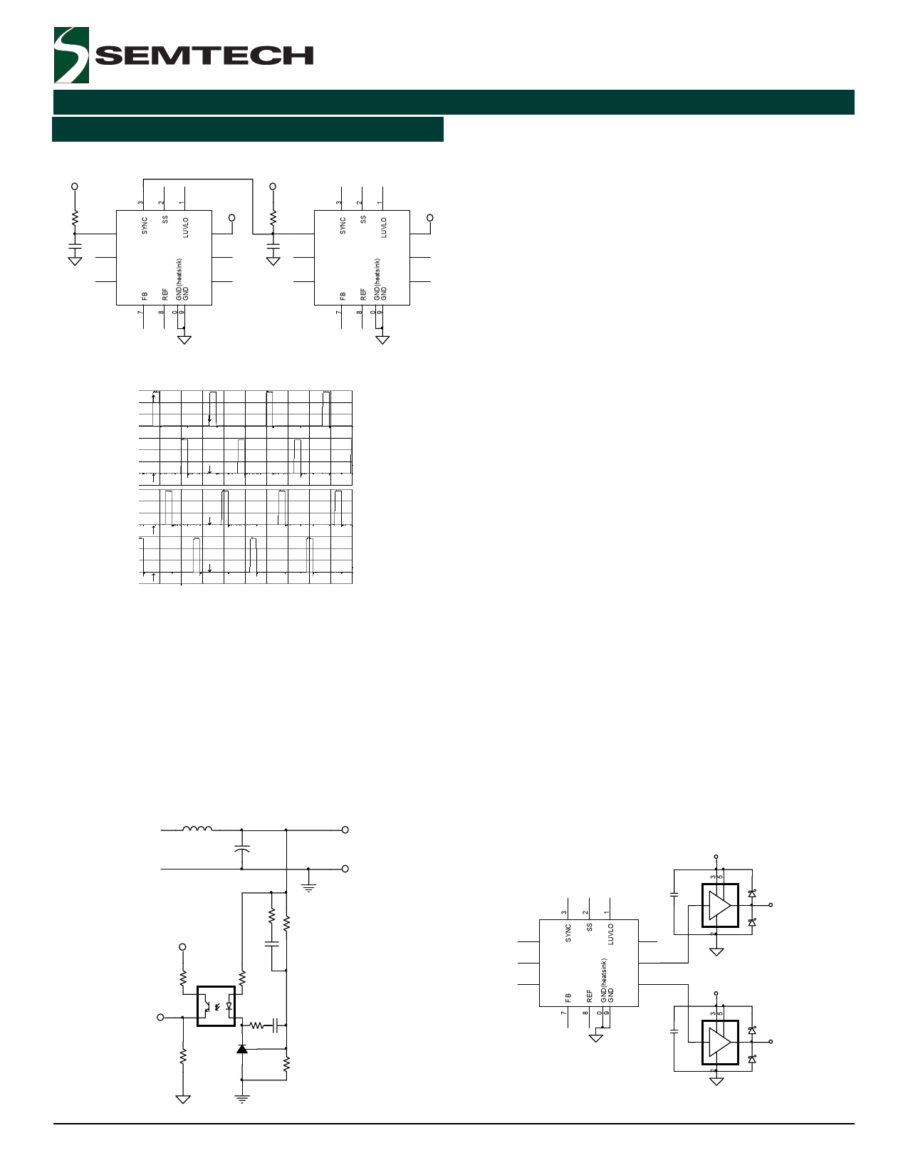
The signal at the FB pin is then compared to the 3X sig-
nal from the current sense/ slope compensation RAMP
pin. Matched out of phase signals are generated to con-
trol the OUTA and OUTB gate drives of the two phases. A
single ramp signal is used to generate the control signals
for both phases, hence achieving a tightly matched per
phase operation.
Voltages below 1.5V at the FB pin, will produce a 0%
duty cycle at the OUTA/OUTB gate drives. This offset is to
provide enough head room for the opto coupler used in
isolated applications.
OUTA (PWM1)
OUTB (PWM1)
OUTA (PWM2)
OUTB (PWM2)
FEED BACK
GATE DRIVERS
OUTA and OUTB are out of phase bipolar gate drive out-
put stages, that are supplied from VCC and provide a
peak source/sink current of about 100mA. Both stages
are capable of driving the logic input of external MOSFET
drivers or a NPN/PNP transistor buffer. The output stages
switch at half the oscillator frequency. When the voltage
on the RC pin is rising, one of the two outputs is high, but
during fall time, both outputs are off. This “dead time”
between the two outputs, along with a slower output rise
and fall time, insures that the two outputs can not be on
at the same time. The dead time is programmable and
depends upon the timing capacitor.
The error signal from output of an external error ampli-
fier such as SC431 or SC4431 is applied to the inverting
input of the PWM comparator at the FB pin either di-
rectly or via an opto-coupler for the isolated applications.
For best stability, keep the FB trace length as short as
possible.
+Vo
It should be noted that if high speed/high current drivers
such as the SC1301 are used, careful layout guide lines
must be followed in order to minimize stray inductance,
which might cause negative voltages at the output of
the drivers. This negative voltage can be clamped to a
reasonable level by placing a small Schottky diode di-
rectly at the output of the driver as shown below:
Lo1
+
Co1
REF
FB
SC431
-Vo
4 RC
5 ILIM
6 RAMP
VCC
S C 4806
VCC 12
OUTA 11
OUTB 10
D_B1
1
4
Gate_A
D_B2
SC1301A
VCC
D_A1
1
4
Gate_B
D_A2
SC1301A
2006 Semtech Corp.
10
www.semtech.com
Share Link: 