SC480EVB Просмотр технического описания (PDF) - Semtech Corporation
Номер в каталоге
Компоненты Описание
производитель
SC480EVB Datasheet PDF : 25 Pages
| |||
SC480
POWER MANAGEMENT
Electrical Characteristics (Cont.)
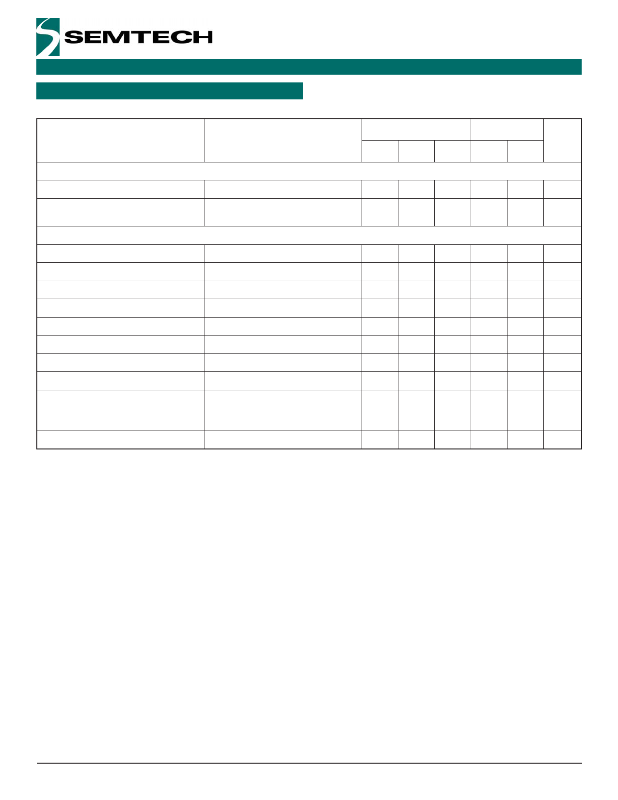
TEST CONDITIONS: VIN = 15V, VCCA = VDDP = VTTEN = EN/PSV = 5V, VDDQ = VTTIN = 1.8V, RTON = 1MΩ. TAMB = -40 TO +85C.
Parameter
Conditions
25°C
Min Typ Max
-40°C to 85°C
Min Max
Units
FB Input Thresholds
FB Logic Input Low
VDDQ Set for 2.5V (DDR1)
0.3
V
VCCA
FB Logic Input High
VDDQ Set for 1.8V (DDR2)
- 0.7
V
Gate Drives
Shoot-Thru Protection Delay(4)(7)
DH or DL Rising
30
ns
DL Pull-Down Resistance
DL Low
0.8
Ω
DL Sink Current
VDL = 2.5V
3.1
A
DL Pull-Up Resistance
DL High
2
Ω
DL Source Current
VDL = 2.5V
1.3
A
DH Pull-Down Resistance
DH Low, BST - LX = 5V
2
Ω
DH Pull-Up Resistance(8)
DH High, BST - LX = 5V
2
Ω
DH Sink/Source Current
VDH = 2.5V
1.3
A
VTT Pull-Up Resistance
VTTS < REF
0.25
Ω
VTT Pull-Down Resistance
VTTS > REF
0.25
Ω
VTT Peak Sink/Source Current(9)
3.6
2.0
A
Notes:
1) The VDDQ DC regulation level is higher than the FB error comparator threshold by 50% of the ripple voltage.
2) Using a current sense resistor, this measurement relates to PGND1 minus the source of the low-side MOSFET.
3) clks = switching cycles, consisting of one high side and one low side gate pulse.
4) Guaranteed by design.
5) Thermal shutdown latches both outputs (VTT and VDDQ) off, requiring VCCA or EN/PSV cycling to reset.
6) VTT soft-start ramp rate is limited to 5.5mV/μs typical. If the VDDQ/2 ramp rate is slower than 5.5mV/μsec, the VTT soft-start ramp will follow the VDDQ/2
ramp.
7) See Shoot-Through Delay Timing Diagram on Page 6.
8) Semtech’s SmartDriver™ FET drive first pulls DH high with a pull-up resistance of 10Ω (typ.) until LX = 1.5V (typ.). At this point, an additional pull-up device is
activated, reducing the resistance to 2Ω (typical). This creates a softer turn-on with minimal power loss, eliminating the need for an external gate or boost
resistor.
9) Provided operation below TJ(MAX) is maintained. VTT output current is also limited by internal MOSFET resistance which is typically 0.25Ω at 25°C and which
increases with temperature, and by available source voltage (typically VDDQ/2).
© 2006 Semtech Corp.
5
www.semtech.com
Share Link: 