SC4524A Просмотр технического описания (PDF) - Semtech Corporation
Номер в каталоге
Компоненты Описание
производитель
SC4524A Datasheet PDF : 19 Pages
| |||
SC4524A
Applications Information (Cont.)
As the load draws more current from the regulator, the
current-limit comparator ILIM (Figure 2) will eventually
limit the switch current on a cycle-by-cycle basis. The
over-current signal OC goes high, setting the latch B3. The
soft-start capacitor is discharged with (ID - IC) (Figure 3). If
the inductor current falls below the current limit and the
PWM comparator instead turns off the switch, then latch
B3 will be reset and IC will recharge the soft-start capacitor.
If over-current condition persists or OC becomes asserted
more often than PWM over a period of time, then the
soft-start capacitor will be discharged below 1.9V. At this
juncture, comparator B4 sets the overload latch B2. The
soft-start capacitor will be continuously discharged with
(ID - IC). The COMP pin is immediately pulled to ground. The
switching regulator is shut off until the soft-start capacitor
is discharged below 1.0V. At this moment, the overload
latch is reset. The soft-start capacitor is recharged and
Fig.4 the converter again undergoes soft-start. The regulator
will go through soft-start, overload shutdown and restart
until it is no longer overloaded.
If the FB voltage falls below 0.8V because of output
overload, then the switching frequency will be reduced.
Frequency foldback helps to limit the inductor current
when the output is hard shorted to ground.
During normal operation, the soft-start capacitor is
charged to 2.4V.
Setting the Output Voltage
The regulator output voltage is set with an external
resistive divider (Figure 1) with its center tap tied to the
FB pin. For a given R6 value, R4 can be found by
R 4 = R6 V.0OV −
(1)
SettingDt=he SwVitOc+hiVnDg Frequency
VIN + VD − VCESAT
The switching frequency of the SC4524A is set with an
external resistor from the ROSC pin to ground.
MinimuDmIL =On(VTOim+FeSVWDC)⋅o⋅Ln(si−dDer)ation
The
opLera=ti(nVg2O
+duVDty) ⋅
0 % ⋅ IO
(cyc−leD)
⋅ FS W
of
a
non-synchronous
step-
downR4sw=iRtc6hingV.0OVre−gulator in continuous-conduction
mode (CCM) is given by
D = VIN +VVOD+−V VDCESAT
(2)
where VCESAT is the switch saturation voltage and VD is
voltage drop across the rectifying diode.
In
DIL
peak
= (VO + VD ) ⋅ (
currentF-mSWo⋅dLe
− D)
control,
the
PWM
modulating
ramp is the sensed current ramp of the power switch.
Tohni.sTchuLerrine=nte(trVsr2Oae0m+c%tVpioD⋅nIi)Os⋅
(ab−seDn) t unless the switch is turned
o⋅FfStWhis ramp with the output of the
voltage feedback error amplifier determines the switch
pulse width. The propagation delay time required to
immedIRiaMtSe_lCyINtu=rInOo⋅ ff Dth⋅e(sw−iDtc)h after it is turned on is the
minimum controllable switch on time (TON(MIN)).
AC =
AC =
R7 =
C5 =
C8 =
Vo =
Vc
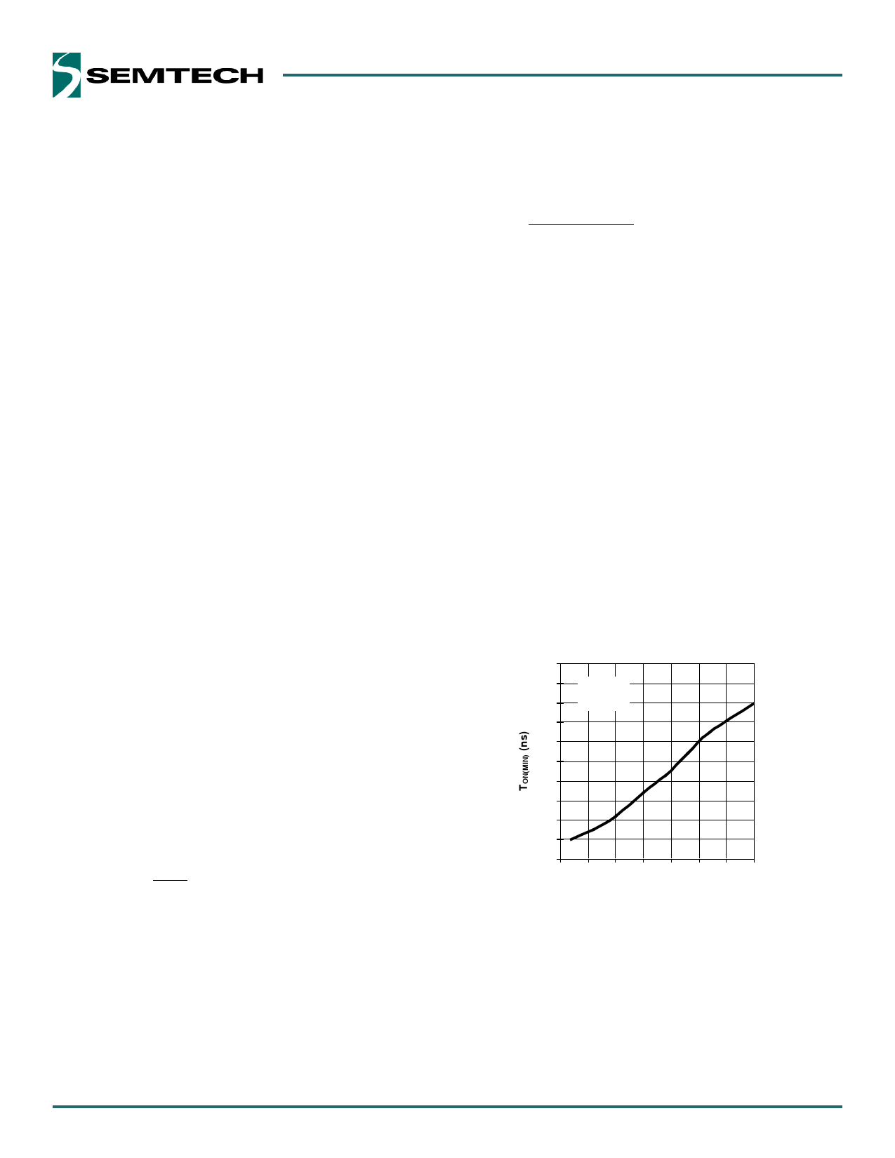
Closed-loop measurement shows that the SC4524A
m(FiignuimreDu4mV)O.
oI=fnDthtILiem⋅reeEqiSsuRiareb+do8us⋅twF1iSt3Wc5h⋅nCosOnattirmoeomis
temperature
shorter than
the minimum on time, the regulator will either skip cycles
or it will jitter.
SS270 REV 6-7
GPWM
R7 =
CIN
>
4
200
IO
M⋅ DinVimINu⋅mFSOWn
Time
vs Temperature
C5 =
190
VO =1.5V
180
1MHz
170
C8 =
160
150
140
130
AC
=
−
20
⋅
l111o012g000
GCAR
S
⋅
2πFCC O
⋅
VFB
VO
-50 -25 0 25 50 75 100 125
AC
=
−
20
⋅
log
28
⋅
6.Te⋅ m0pe−r3atu⋅r2e
(OC)
π ⋅ 80
⋅
0 3
⋅ 22 ⋅0 −6
⋅ .0 = 5
3.3
Figure 4. Variation of Minimum On Time
5.9 with Ambient Temperature
RTo7
=all0o.w28f0o⋅r20t0ra−n3 s=ie2n2t
.3k
headroom,
the
minimum
operating
Csthw5ei=twc2hoπros⋅nt-tc6iam⋅see0msh3ion⋅ 2uiml2du.bme⋅oa0tn3letia=ms0te2..405%nFto 30% higher than
C8
=
2
π⋅
600
⋅
03
⋅ 22. ⋅0 3
= 2pF
10
Share Link: 