SA5211 Просмотр технического описания (PDF) - Philips Electronics
Номер в каталоге
Компоненты Описание
производитель
SA5211 Datasheet PDF : 28 Pages
| |||
Philips Semiconductors
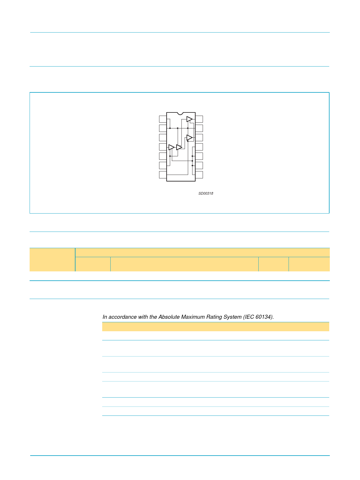
4. Pinning information
4.1 Pinning
SA5211
Transimpedance amplifier (180 MHz)
Fig 1. Pin configuration.
5. Ordering information
D Package
GND2 1
GND2 2
NC 3
IIN 4
NC 5
VCC1 6
VCC2 7
14 OUT (–)
13 GND2
12 OUT (+)
11 GND1
10 GND1
9 GND1
8 GND1
TOP VIEW
SD00318
Table 1: Ordering information
Type number Package
Name
Description
SA5211D
SO14
plastic small outline package; 14 leads; body width 3.9 mm
Version Temperature
range (°C)
SOT108-1 −40 to +85
6. Limiting values
Table 2: Limiting values
In accordance with the Absolute Maximum Rating System (IEC 60134).
Symbol Parameter
Conditions
Min
Max
VCC
Tamb
power supply
operating ambient
temperature range
−
6
-40
+85
TJ
operating junction
temperature range
-55
+150
TSTG
PD MAX
storage temperature range
power dissipation, TA = 25 °C
(still-air) [1]
-65
+150
−
1.0
IIN MAX
θJA
maximum input current [2]
thermal resistance
−
5
−
125
Unit
V
°C
°C
°C
W
mA
°C/W
[1] Maximum dissipation is determined by the operating ambient temperature and the thermal resistance:
θJA = 125 °C/W
[2] The use of a pull-up resistor to VCC, for the PIN diode is recommended.
9397 750 07427
Product specification
Rev. 03 — 07 October 1998
© Philips Electronics N.V. 2001. All rights reserved.
2 of 28
Share Link: 